
MARKET INSIGHTS
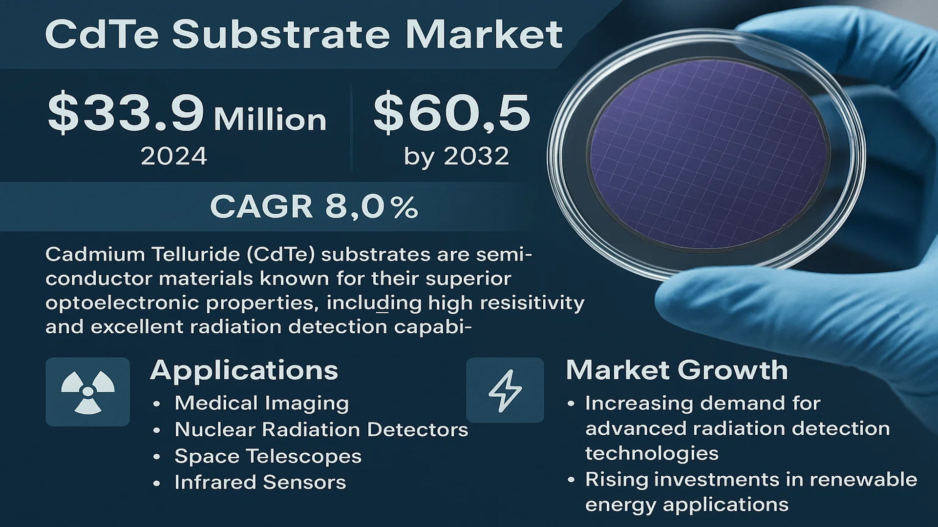
The global CdTe Substrate Market was valued at 33.9 million in 2024 and is projected to reach US$ 60.5 million by 2032, at a CAGR of 8.0% during the forecast period.
Cadmium Telluride (CdTe) substrates are semiconductor materials known for their superior optoelectronic properties, including high resistivity and excellent radiation detection capabilities. These substrates are widely used in medical imaging (CT and PET scanners), nuclear radiation detectors, space telescopes, and infrared sensors due to their ability to operate efficiently at room temperature. The material’s wide bandgap makes it particularly suitable for high-energy radiation detection applications, where precision and reliability are critical.
The market growth is driven by increasing demand for advanced radiation detection technologies across medical, industrial, and defense sectors. Additionally, rising investments in renewable energy applications, such as thin-film solar cells, are contributing to market expansion. Key players like II-VI Incorporated and 5N Plus are actively developing high-purity CdTe substrates to meet the growing industry requirements, further accelerating market progress. However, challenges such as material toxicity and high production costs may hinder widespread adoption in certain applications.
MARKET DYNAMICS
MARKET DRIVERS
Growing Demand for High-Efficiency Photovoltaic Applications to Drive Market Expansion
The global push toward renewable energy sources is accelerating the adoption of cadmium telluride (CdTe) substrates in photovoltaic applications. CdTe thin-film solar panels demonstrate superior performance in real-world conditions with 22.1% module efficiency, surpassing many conventional silicon-based alternatives. Their ability to perform better in high-temperature and low-light environments makes them ideal for utility-scale solar farms, stimulating investment from energy providers. With solar energy capacity projected to grow at 8-10% annually through 2030, the demand for CdTe substrates is expected to increase in tandem as manufacturers scale up production to meet this surging demand.
Advancements in Medical Imaging Technologies Fueling Adoption
Medical imaging represents one of the fastest-growing application segments for CdTe substrates due to their excellent X-ray and gamma-ray detection capabilities. The global medical imaging market has shown consistent 6-7% annual growth, with digital radiography and nuclear medicine applications leading the charge. CdZnTe (CZT) detectors offer superior energy resolution compared to traditional scintillation detectors, enabling more accurate diagnostics while reducing patient radiation exposure. Major healthcare providers are increasingly adopting CZT-based SPECT and PET scanners that provide high-quality images at lower radiation doses, creating sustained demand for high-purity CdTe substrates.
➤ The U.S. FDA’s recent clearance of several CZT-based cardiac imaging systems demonstrates the technology’s growing acceptance in clinical applications.
Increasing Defense and Space Applications Create New Demand
National security investments in radiation detection and space exploration are generating strong demand for radiation-hardened CdTe substrates. Modern satellite constellations and deep space probes require reliable detectors for cosmic radiation monitoring and astronomical observations. Defense applications including border security and nuclear threat detection systems increasingly utilize CZT-based detectors due to their room-temperature operation and high sensitivity. With global defense budgets exceeding $2 trillion annually and space agencies planning numerous interplanetary missions, these sectors will continue driving technological innovation and substrate quality improvements in the CdTe market.
MARKET CHALLENGES
Material Purity and Crystal Defects Pose Manufacturing Hurdles
Despite their advantages, CdTe substrates face significant production challenges related to material purity and crystalline perfection. Even minor impurities can drastically reduce detector performance, requiring manufacturers to maintain extremely tight control over material composition. The Czochralski process used for single crystal growth often results in defects that degrade electrical properties, with typical yield rates below 60% for premium-grade material. These manufacturing difficulties contribute to higher production costs compared to conventional semiconductor materials, limiting broader adoption in cost-sensitive applications.
Other Challenges
Supply Chain Vulnerabilities
The CdTe substrate market remains vulnerable to supply chain disruptions for tellurium, a relatively rare byproduct of copper refining. With approximately 90% of tellurium production concentrated in just five countries, geopolitical factors can create supply instability and price volatility. Recent trade restrictions have caused tellurium prices to fluctuate by as much as 35% year-over-year, complicating production planning and inventory management for substrate manufacturers.
Health and Environmental Concerns
Regulatory scrutiny of cadmium-containing materials continues to influence market dynamics. While CdTe in finished products poses minimal risk, manufacturing facilities must implement rigorous safety protocols to prevent cadmium exposure. Environmental agencies in multiple regions are evaluating stricter controls on material handling and disposal, potentially increasing compliance costs. These factors may slow market expansion in regions with particularly stringent environmental regulations.
MARKET RESTRAINTS
High Production Costs Limit Market Penetration
The specialized equipment and controlled environments required for CdTe substrate manufacturing result in significantly higher production costs compared to conventional semiconductors. A single crystal growth furnace for 6-inch CZT wafers can exceed $2 million, while the purification process requires additional capital-intensive infrastructure. These economic barriers discourage new market entrants and limit production scale-up, keeping substrate prices at premium levels. Cost-sensitive applications often opt for lower-performance alternatives despite CdTe’s technical advantages, particularly in price-driven emerging markets.
Limited Wafer Size Constrains Device Integration
CdTe substrate technology currently faces physical limitations in wafer size scaling, with most commercial production limited to 4-6 inch diameters. This contrasts sharply with silicon wafer standards that have reached 12-inch diameters, enabling more economical device integration. The smaller wafer sizes increase manufacturing complexity and cost when producing large-area detectors or solar panels, as more substrates must be assembled to achieve the required surface area. Research institutions and manufacturers are actively working on scaling technologies, but progress has been incremental due to the material’s crystalline growth challenges.
MARKET OPPORTUNITIES
Emerging Nuclear Security Applications Present Growth Potential
Global concern over nuclear proliferation and radioactive material detection is creating new opportunities for CdTe substrates in security applications. Airports, seaports, and border crossings worldwide are upgrading radiation monitoring infrastructure, with advanced spectroscopic detectors becoming the standard for threat identification. Modern systems utilizing CZT can distinguish between naturally occurring radioactive materials and potential threats with over 95% accuracy, driving adoption by security agencies. With governments allocating increased funding for nuclear security infrastructure, this segment represents one of the most promising growth avenues for substrate manufacturers.
Research into Quantum Technologies Opens New Possibilities
Cutting-edge research in quantum sensing and computing is revealing new potential applications for CdTe substrates. Several quantum computing architectures are exploring the use of CdTe-based qubits due to their long coherence times at elevated temperatures. Meanwhile, defense researchers are developing quantum-enhanced imaging systems using CZT detectors that could revolutionize night vision and through-wall imaging. While these applications remain in early development stages, successful commercialization could create entirely new market segments for CdTe substrates beyond traditional radiation detection uses.
Expansion in Emerging Economies Offers Untapped Potential
Developing nations present significant untapped opportunities as they modernize healthcare infrastructure and expand renewable energy capacity. Countries in Southeast Asia and Africa are investing heavily in solar energy projects where CdTe thin-film technology could be particularly advantageous due to better performance in hot climates. Simultaneously, hospital networks across these regions are upgrading diagnostic imaging capabilities, creating demand for advanced X-ray and nuclear medicine equipment. Strategic partnerships between substrate manufacturers and local system integrators could accelerate market penetration in these growth regions.
CdTe SUBSTRATE MARKET TRENDS
Increasing Demand for High-Performance Radiation Detection Drives Market Growth
The global CdTe (Cadmium Telluride) substrate market is experiencing robust growth, primarily fueled by its extensive use in radiation detection and imaging applications. The material’s high resistivity, wide bandgap, and excellent detection efficiency make it indispensable in medical imaging systems, such as CT and PET scanners. With nuclear medicine and advanced diagnostics witnessing significant advancements, the demand for CdTe substrates is projected to surge, especially in regions with expanding healthcare infrastructure. The market was valued at $33.9 million in 2024 and is expected to reach $60.5 million by 2032, growing at a CAGR of 8.0% during the forecast period.
Other Trends
Expansion in Space and Defense Applications
CdTe substrates are increasingly adopted in space telescopes and satellite imaging systems due to their ability to operate at room temperature while maintaining high performance. Governments and aerospace agencies are investing heavily in next-generation infrared sensors for surveillance and astronomical research, boosting the demand for high-quality Single Crystal CdZnTe (CZT) substrates. The U.S. and China, leading in defense and space technology expenditure, are driving a substantial portion of this demand.
Technological Innovations in Optoelectronics
The integration of CdTe substrates in optoelectronic devices, including infrared detectors and photovoltaic cells, has opened new growth avenues. Research in semiconductors and energy-efficient solutions has heightened the focus on polycrystalline CZT substrates, particularly in solar energy and industrial automation. The shift towards next-generation X-ray detectors, which rely on CdTe for superior resolution and sensitivity, further underscores the market’s potential. Leading manufacturers such as II-VI Incorporated and 5N Plus are actively expanding their production capacities to meet the rising industrial and medical demands.
COMPETITIVE LANDSCAPE
Key Industry Players
Innovation and Expansion Strategies Drive Market Competition
The global CdTe substrate market features a semi-consolidated competitive landscape, where leading manufacturers compete based on product innovation, material quality, and application-specific solutions. JX Advanced Metals Corporation and II-VI Incorporated are among the dominant players, collectively holding a significant revenue share as of 2024. These companies leverage their expertise in semiconductor materials to cater to high-growth sectors like medical imaging and industrial radiation detection.
MTI Corporation and 5N Plus have strengthened their positions through strategic collaborations and continuous R&D investments. MTI, for instance, has expanded its production capacity in Asia to meet rising demand from electronics manufacturers. Meanwhile, 5N Plus focuses on high-purity CdTe substrates, targeting niche applications in space telescopes and defense systems.
Regional players such as Shaanxi Imdetek Co., Ltd. (China) and Eurorad S.A. (France) are gaining traction by offering cost-effective alternatives without compromising material performance. Their growth is further propelled by local government incentives supporting domestic semiconductor production.
Recent developments include PAM-XIAMEN‘s breakthrough in single-crystal CZT substrates, enhancing energy resolution for gamma-ray detectors. Similarly, Wuhan Tuocai Technology has introduced polycrystalline CdTe substrates optimized for solar cell applications — a segment projected to grow at a 7.9% CAGR from 2024–2032.
List of Key CdTe Substrate Manufacturers
- JX Advanced Metals Corporation (Japan)
- II-VI Incorporated (U.S.)
- MTI Corporation (U.S.)
- 5N Plus (Canada)
- Eurorad S.A. (France)
- Shaanxi Imdetek Co., Ltd. (China)
- PAM-XIAMEN (China)
- Wuhan Tuocai Technology Co., Ltd. (China)
- Kinheng Crystal (China)
- CapeSym (U.S.)
- Shalom EO (Israel)
Segment Analysis:
By Type
Single Crystal CZT Segment Holds Largest Share Due to Superior Performance in Radiation Detection
The market is segmented based on type into:
- Single Crystal CZT
- Polycrystalline CZT
- Others
By Application
Medical Segment Leads Market Adoption Driven by Radiation Imaging and Diagnostic Applications
The market is segmented based on application into:
- Electronics & Semiconductors
- Industrial
- Energy
- Medical
- Others
By Substrate Size
Standard Size Substrates Dominate for Compatibility with Existing Manufacturing Processes
The market is segmented based on substrate size into:
- Below 10mm thickness
- 10-20mm thickness
- Above 20mm thickness
By End-Use Industries
Healthcare Sector Shows Strongest Growth Potential Due to Increasing Medical Imaging Demands
The market is segmented based on end-use industries into:
- Healthcare
- Aerospace & Defense
- Nuclear Power
- Research Institutions
Regional Analysis: CdTe Substrate Market
North America
North America leads the global CdTe substrate market, driven by robust demand from the medical imaging sector, particularly in CT and PET scanner manufacturing. The U.S. dominates regional growth, supported by substantial R&D investments in radiation detection technologies and a well-established semiconductor industry. Stringent regulations for medical device safety and nuclear non-proliferation initiatives further propel the adoption of high-quality single crystal CZT substrates. Key players like II-VI Incorporated and CapeSym have a strong presence, leveraging partnerships with national laboratories and aerospace contractors. However, reliance on cadmium—a regulated material—poses compliance challenges for manufacturers navigating EPA and OSHA standards.
Asia-Pacific
The Asia-Pacific region is experiencing the fastest CAGR (estimated at 9.2%) due to expanding electronics manufacturing hubs in China, Japan, and South Korea. China’s dominance in semiconductor production and government-backed initiatives like the National Key R&D Program foster local CdTe substrate development for infrared sensors and space applications. While cost-efficient polycrystalline CZT substrates are preferred for industrial applications, Japan maintains leadership in high-purity single crystal production for medical imaging. Challenges include intellectual property disputes and inconsistent raw material quality, though domestic players like Shaanxi Imdetek and PAM-XIAMEN are gaining traction through vertical integration.
Europe
Europe’s market growth revolves around nuclear safety applications and renewable energy projects, particularly in Germany and France. Eurorad S.A. and 5N Plus supply specialized CdTe substrates for gamma-ray spectrometers used in nuclear facility monitoring. The region benefits from Horizon Europe funding for radiation-hardened electronics but faces constraints due to REACH regulations limiting cadmium usage. Sustainability-driven R&D focuses on recycling spent substrates, with Fraunhofer institutes pioneering closed-loop material recovery systems. Market expansion remains moderate, hindered by preference for silicon-based alternatives in consumer electronics.
Middle East & Africa
This emerging market shows niche potential in oil & gas pipeline monitoring and border security applications. Israel leads technological adoption through partnerships with defense contractors utilizing CdTe-based radiation portals. The UAE’s space program has created sporadic demand for satellite-grade substrates, though reliance on imports persists due to limited local manufacturing capabilities. Growth is tempered by geopolitical instability and underdeveloped healthcare infrastructure, restricting medical imaging applications. Recent joint ventures between Turkish universities and European suppliers aim to build regional testing facilities.
South America
South America’s market remains nascent, with Brazil accounting for over 60% of regional demand—primarily for industrial thickness gauges and academic research. Argentina’s nuclear energy program sporadically sources radiation detection substrates, but economic volatility disrupts procurement cycles. The lack of indigenous production facilities forces dependence on North American and Asian imports, often at premium costs. Mining safety regulations in Chile present untapped opportunities, though adoption rates lag behind global averages due to budgetary constraints in extractive industries.
Report Scope
This market research report provides a comprehensive analysis of the global CdTe Substrate market, covering the forecast period 2024–2032. It offers detailed insights into market dynamics, technological advancements, competitive landscape, and key trends shaping the industry.
Key focus areas of the report include:
- Market Size & Forecast: Historical data and future projections for revenue, unit shipments, and market value across major regions and segments. The global CdTe Substrate market was valued at USD 33.9 million in 2024 and is projected to reach USD 60.5 million by 2032, growing at a CAGR of 8.0%.
- Segmentation Analysis: Detailed breakdown by product type (Single Crystal CZT, Polycrystalline CZT, Others), application (Electronics & Semiconductors, Industrial, Energy, Medical, Others), and end-user industry to identify high-growth segments and investment opportunities.
- Regional Outlook: Insights into market performance across North America (U.S., Canada, Mexico), Europe (Germany, France, U.K.), Asia-Pacific (China, Japan, South Korea), and other regions, including country-level analysis where relevant.
- Competitive Landscape: Profiles of leading market participants, including JX Advanced Metals Corporation, II-VI Incorporated, 5N Plus, MTI Corporation, and Shaanxi Imdetek Co., Ltd., covering their product offerings, R&D focus, and recent developments.
- Technology Trends & Innovation: Assessment of emerging semiconductor technologies, fabrication techniques, and evolving industry standards in CdTe substrate applications.
- Market Drivers & Restraints: Evaluation of factors driving market growth along with challenges, supply chain constraints, and regulatory issues in the semiconductor materials sector.
- Stakeholder Analysis: Insights for component suppliers, OEMs, system integrators, investors, and policymakers regarding the evolving ecosystem and strategic opportunities.
Primary and secondary research methods are employed, including interviews with industry experts, data from verified sources, and real-time market intelligence to ensure the accuracy and reliability of the insights presented.
FREQUENTLY ASKED QUESTIONS:
What is the current market size of Global CdTe Substrate Market?
-> CdTe Substrate Market was valued at 33.9 million in 2024 and is projected to reach US$ 60.5 million by 2032, at a CAGR of 8.0% during the forecast period.
Which key companies operate in Global CdTe Substrate Market?
-> Key players include JX Advanced Metals Corporation, MTI Corporation, II-VI Incorporated, 5N Plus, and Shaanxi Imdetek Co., Ltd., among others.
What are the key growth drivers?
-> Key growth drivers include increasing demand for medical imaging devices, nuclear radiation detectors, and space applications, along with technological advancements in semiconductor materials.
Which region dominates the market?
-> North America currently leads in market share, while Asia-Pacific is expected to witness the fastest growth during the forecast period.
What are the emerging trends?
-> Emerging trends include development of high-purity CdTe substrates, integration with AI-based imaging systems, and expansion in space telescope applications.

Get Sample Report PDF for Exclusive Insights
Report Sample Includes
- Table of Contents
- List of Tables & Figures
- Charts, Research Methodology, and more...






