MARKET INSIGHTS
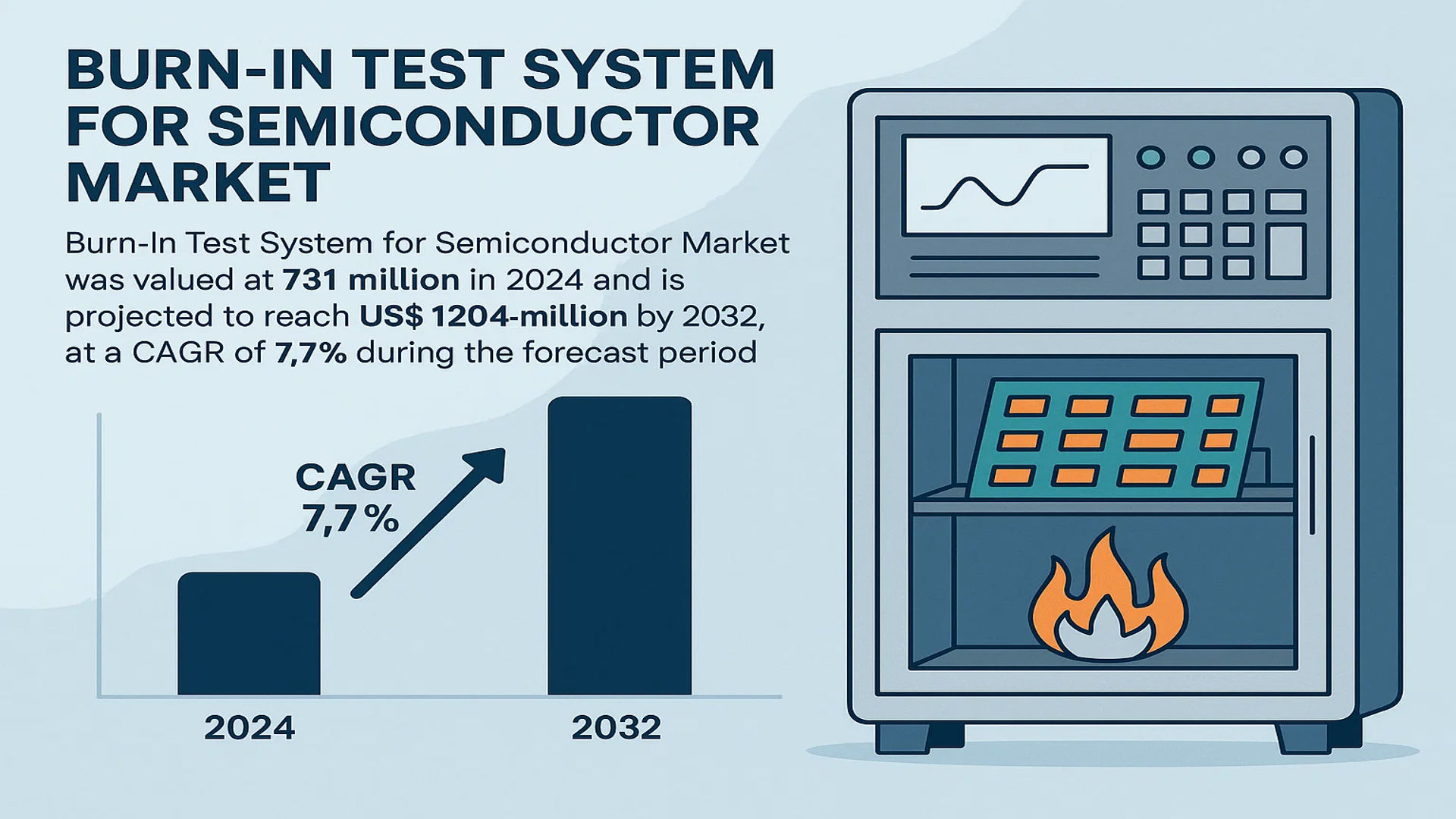
The global Burn-In Test System for Semiconductor Market was valued at 731 million in 2024 and is projected to reach US$ 1204 million by 2032, at a CAGR of 7.7% during the forecast period.
A Burn-In Test System for Semiconductor is specialized equipment designed to test the reliability and durability of semiconductor devices over extended periods. These systems perform aging tests by subjecting semiconductor components to specific, elevated stress conditions—such as high temperature, voltage, and power cycling—to accelerate the appearance of potential defects and analyze changes in load capacity and performance. This process is crucial for ensuring the reliability of semiconductor components before they are integrated into final products or systems.
The market is experiencing robust growth driven by the increasing complexity and miniaturization of semiconductor devices, alongside rising demand from high-stakes industries like automotive, telecommunications, and medical devices, where component failure can have severe consequences. Furthermore, the expansion of the Internet of Things (IoT) and artificial intelligence (AI) applications is fueling the need for more rigorous reliability testing. Key players such as Advantest, Aehr Test Systems, and ESSPEC are actively innovating, with recent developments including more energy-efficient systems and integration with smart factory automation to meet the evolving demands of semiconductor manufacturers globally.
MARKET DYNAMICS
MARKET DRIVERS
Growing Demand for High-Reliability Semiconductors in Automotive and Medical Sectors to Drive Market Growth
The automotive industry’s rapid shift toward electric and autonomous vehicles is significantly increasing the demand for highly reliable semiconductor components. Modern vehicles incorporate over 3,000 semiconductor chips per unit, with advanced driver-assistance systems (ADAS) and electric powertrains requiring zero-defect performance. Burn-in test systems are critical for identifying early-life failures in these components, ensuring they withstand extreme temperature ranges from -40°C to 150°C and maintain functionality under vibration and power cycling conditions. Similarly, the medical device sector requires absolute reliability for implantable devices and diagnostic equipment, where component failure could have life-threatening consequences. This heightened quality requirement across safety-critical applications is driving increased adoption of advanced burn-in testing systems globally.
Expansion of 5G Infrastructure and IoT Devices to Accelerate Market Adoption
The global rollout of 5G networks and proliferation of Internet of Things (IoT) devices is creating substantial demand for robust semiconductor testing solutions. 5G base stations require semiconductors that can operate continuously under high thermal loads, while IoT devices often operate in uncontrolled environments where reliability is paramount. The number of connected IoT devices is projected to exceed 29 billion by 2030, each containing multiple semiconductor components that require thorough reliability testing. Burn-in systems help manufacturers identify potential field failures before deployment, reducing warranty claims and maintaining brand reputation. Telecommunications infrastructure providers are particularly demanding rigorous testing protocols, as network downtime costs can exceed $300,000 per hour for major carriers, making component reliability a critical business consideration.
Increasing Complexity of Semiconductor Designs to Fuel Advanced Testing Requirements
Semiconductor manufacturers are developing increasingly complex designs with smaller process nodes, 3D packaging, and heterogeneous integration, creating new challenges for reliability testing. Advanced nodes below 7nm exhibit different failure mechanisms compared to traditional components, requiring more sophisticated burn-in testing methodologies. The transition to 3D NAND flash memory and advanced packaging technologies like chiplets has increased the importance of thermal management during testing, as these structures generate significant heat density. Modern burn-in systems must accommodate these complexities while maintaining testing throughput, driving innovation in temperature control, power delivery, and test pattern generation. This technological evolution is pushing manufacturers to upgrade their testing infrastructure with systems capable of handling these advanced semiconductor architectures.
MARKET CHALLENGES
High Capital Investment and Operational Costs to Challenge Market Penetration
The significant capital expenditure required for advanced burn-in test systems presents a substantial barrier to market entry and expansion. A single high-end burn-in system can cost between $500,000 to $2 million, depending on configuration and capabilities, while complete testing facilities require multiple systems supported by environmental controls and automation. Operational expenses include substantial energy consumption for thermal management, maintenance costs for sophisticated instrumentation, and facility requirements for temperature and humidity control. These financial barriers are particularly challenging for small and medium-sized semiconductor companies and testing service providers, limiting their ability to compete with larger players who can achieve economies of scale in their testing operations.
Other Challenges
Technical Complexity in Testing Advanced Semiconductor Packages
The increasing complexity of semiconductor packaging, including 2.5D and 3D integration, system-in-package designs, and heterogeneous integration, creates significant technical challenges for burn-in testing. These advanced packages require specialized fixtures, thermal management solutions, and test methodologies that can accommodate multiple die with different power requirements and thermal characteristics. The testing infrastructure must address issues such as thermal interface materials degradation, interposer reliability, and power delivery network stability under accelerated aging conditions. Developing comprehensive test solutions for these complex packages requires extensive research and development investment, creating delays in market availability of appropriate testing equipment.
Throughput and Productivity Pressures
Semiconductor manufacturers face constant pressure to reduce testing time and increase throughput while maintaining comprehensive reliability assessment. The burn-in process typically requires 24 to 168 hours of continuous operation per device lot, creating production bottlenecks. Manufacturers must balance the need for thorough reliability testing with production schedule requirements, leading to difficult trade-offs between test coverage and time-to-market. This challenge is exacerbated by the increasing number of devices requiring testing and the growing complexity of test protocols, forcing manufacturers to invest in parallel testing capabilities and automation, which further increases capital requirements.
MARKET RESTRAINTS
Technical Limitations in Testing Emerging Semiconductor Technologies to Restrain Market Growth
Emerging semiconductor technologies, including wide bandgap materials like silicon carbide and gallium nitride, present unique testing challenges that current burn-in systems are not fully equipped to handle. These materials operate at higher temperatures, voltages, and switching frequencies than traditional silicon devices, requiring specialized testing conditions that existing equipment cannot reliably provide. The testing infrastructure must accommodate voltage requirements exceeding 1,200 volts and temperature ranges beyond 200°C, necessitating completely redesigned chamber architectures, power supplies, and safety systems. This technological gap creates a significant restraint as manufacturers of these advanced semiconductors cannot adequately validate their products’ reliability, potentially slowing adoption in critical applications such as electric vehicle power systems and renewable energy infrastructure.
Additionally, the industry faces challenges in developing appropriate failure criteria and acceleration factors for these new materials. Traditional Arrhenius models used for silicon devices may not accurately predict failure mechanisms in wide bandgap semiconductors, requiring completely new reliability physics models and testing methodologies. This uncertainty in testing protocols makes it difficult to establish industry standards and certification processes, further restraining market growth until these technical challenges are resolved through collaborative research and development efforts across the semiconductor ecosystem.
MARKET OPPORTUNITIES
Integration of Artificial Intelligence and Machine Learning to Create New Testing Paradigms
The integration of artificial intelligence and machine learning technologies presents significant opportunities for enhancing burn-in testing efficiency and effectiveness. AI algorithms can analyze historical test data to optimize test parameters, predict failure patterns, and reduce unnecessary testing time. Machine learning systems can identify subtle patterns in device behavior that might indicate potential reliability issues, enabling more targeted testing approaches. This technological advancement allows manufacturers to move from standardized burn-in protocols to adaptive testing strategies that respond to real-time device performance data, potentially reducing test time by 30-40% while maintaining or improving reliability assessment quality.
Furthermore, AI-powered predictive maintenance capabilities can significantly reduce equipment downtime and improve testing system reliability. These systems can monitor equipment performance indicators and predict component failures before they occur, scheduling maintenance during planned downtime periods. This approach maximizes equipment utilization and reduces unexpected production interruptions, providing substantial operational benefits for high-volume semiconductor manufacturing facilities where testing capacity directly impacts production output and time-to-market for new products.
Expansion of Outsourced Semiconductor Assembly and Test Services to Drive Demand
The growing trend toward outsourcing semiconductor assembly and testing operations creates substantial opportunities for burn-in system manufacturers and service providers. Many semiconductor companies are focusing on their core design and fabrication competencies while relying on specialized partners for back-end processes including testing. This business model requires OSAT providers to maintain state-of-the-art testing capabilities, driving demand for advanced burn-in systems. The OSAT market has been growing at approximately 6-8% annually, with testing services representing a significant portion of this expansion. This growth trajectory creates ongoing demand for new testing equipment and upgrades to existing infrastructure as OSAT providers compete to offer the most comprehensive and efficient testing services to their semiconductor customers.
Additionally, the increasing complexity of semiconductor packages requires specialized expertise and equipment that many semiconductor companies find more economical to outsource rather than develop in-house. This trend is particularly evident in advanced packaging technologies where the testing requirements exceed the capabilities of standard equipment, creating opportunities for providers who can develop and deploy specialized testing solutions for these emerging technologies.
BURN-IN TEST SYSTEM FOR SEMICONDUCTOR MARKET TRENDS
Rising Demand for High-Reliability Semiconductors in Critical Applications
The global burn-in test system market is experiencing significant growth, driven primarily by the escalating demand for highly reliable semiconductors in mission-critical industries. The automotive sector, particularly with the rapid advancement of electric vehicles (EVs) and autonomous driving systems, requires components that can withstand extreme conditions over long operational lifetimes. Similarly, the aerospace, defense, and medical device industries have near-zero tolerance for semiconductor failure. This has propelled the adoption of sophisticated burn-in test systems, which are essential for screening out infant mortality failures by accelerating the aging process of semiconductor devices under controlled stress conditions. The market is projected to grow from its 2024 valuation of $731 million to over $1.2 billion by 2032, reflecting a compound annual growth rate of 7.7%. This growth is not merely quantitative; it is also qualitative, with a marked shift towards systems capable of handling more complex, higher-density integrated circuits and operating at elevated temperatures and voltages that mimic harsh real-world environments.
Other Trends
Integration of AI and Machine Learning for Predictive Analysis
A pivotal trend reshaping the burn-in test landscape is the integration of artificial intelligence and machine learning algorithms into testing systems. While traditional burn-in procedures apply fixed stress conditions for a predetermined duration, AI-enhanced systems can analyze performance data in real-time to dynamically adjust test parameters. This allows for more efficient and targeted stress testing, potentially reducing test times and energy consumption while improving the accuracy of failure prediction. These smart systems can identify subtle patterns and correlations in the data that precede a failure, moving beyond simple pass/fail criteria to a more nuanced understanding of device reliability and long-term performance. This technological evolution is crucial for keeping pace with the increasing complexity of modern semiconductors, where traditional methods may not be sufficient to uncover latent defects.
Expansion into New Semiconductor Materials and Advanced Packaging
The ongoing transition to new semiconductor materials like silicon carbide (SiC) and gallium nitride (GaN), especially for power electronics, is creating new requirements for burn-in test systems. These wide-bandgap semiconductors operate at higher frequencies, temperatures, and power densities than traditional silicon, necessitating burn-in systems that can apply appropriate electrical and thermal stresses. Furthermore, the rise of advanced packaging technologies, such as 2.5D/3D integration and system-in-package (SiP), presents a unique challenge. Burn-in testing must now account for the interactions between multiple heterogeneous dies within a single package, requiring systems with increased pin counts, finer pitch capabilities, and more sophisticated thermal management to ensure the reliability of the entire assembled system, not just individual chips.
COMPETITIVE LANDSCAPE
Key Industry Players
Companies Strive to Strengthen their Product Portfolio to Sustain Competition
The competitive landscape of the global burn-in test system market is moderately fragmented, featuring a mix of established multinational corporations, specialized mid-sized firms, and emerging regional players. Advantest Corporation stands as a dominant force, leveraging its extensive semiconductor test expertise and robust R&D capabilities to maintain a significant market share. Their comprehensive product range, which includes both static and dynamic burn-in systems, caters to high-volume manufacturing environments, particularly for advanced integrated circuits and sensors.
Aehr Test Systems has carved out a substantial niche, especially in the wafer-level and singulated die burn-in segment. Their innovative FOX™ and WaferPak™ technologies address the growing demand for testing complex devices like those used in automotive and AI applications. Similarly, Chroma ATE Inc. holds a strong position, supported by its vertically integrated manufacturing and global service network, which ensures reliable support for clients across North America, Asia, and Europe.
These leading players are actively pursuing growth through strategic initiatives. For instance, recent expansions into new geographical markets and increased investment in developing systems capable of handling higher temperatures and power densities—essential for next-generation semiconductors—are key focus areas. Moreover, partnerships with major semiconductor manufacturers ensure that burn-in systems evolve in tandem with device complexities, such as those required for 5G chips and electric vehicle power modules.
Meanwhile, companies like ESPEC Corp. and Trio-Tech International are strengthening their market presence through targeted R&D and acquisitions. ESPEC’s emphasis on environmental testing chambers integrated with burn-in capabilities provides a competitive edge in reliability testing. Trio-Tech’s diversification into services, including burn-in and test outsourcing, addresses the need for cost-effective solutions among smaller fabricators. These strategies not only enhance their product portfolios but also solidify their roles in an increasingly quality-driven market.
List of Key Burn-In Test System Companies Profiled
- Advantest Corporation (Japan)
- Aehr Test Systems (U.S.)
- Chroma ATE Inc. (Taiwan)
- ESPEC Corp. (Japan)
- Trio-Tech International (U.S.)
- Micro Control Company (U.S.)
- STAr Technologies Inc. (Taiwan)
- KES Systems & Service Inc. (U.S.)
- Hangzhou Changchuan Technology (China)
- Zhejiang Hangke Instrument (China)
Segment Analysis:
By Type
Dynamic Testing Segment Dominates the Market Due to Its Critical Role in Simulating Real-World Operating Conditions
The market is segmented based on type into:
- Static Testing
- Dynamic Testing
By Application
Integrated Circuit Segment Leads Due to High-Volume Manufacturing and Stringent Reliability Requirements
The market is segmented based on application into:
- Integrated Circuit
- Discrete Device
- Sensor
- Optoelectronic Device
By End User
Semiconductor Foundries and IDMs Lead Market Adoption Due to High-Volume Production Needs
The market is segmented based on end user into:
- Semiconductor Foundries
- Integrated Device Manufacturers (IDMs)
- Outsourced Semiconductor Assembly and Test (OSAT) Providers
- Research and Development Institutions
Regional Analysis: Burn-In Test System for Semiconductor Market
Asia-Pacific
The Asia-Pacific region dominates the global burn-in test system market, accounting for over 55% of the total market share. This leadership position is driven by the massive semiconductor manufacturing ecosystems in Taiwan, South Korea, and China. Taiwan Semiconductor Manufacturing Company (TSMC) and Samsung Electronics are key consumers, requiring advanced burn-in systems to ensure the reliability of their cutting-edge nodes, including 5nm and 3nm processes. The region’s growth is further fueled by substantial government investments, such as China’s push for semiconductor self-sufficiency under its “Made in China 2025” initiative. While cost sensitivity remains a factor, the demand for high-volume testing of consumer electronics and automotive chips is insatiable, leading to significant adoption of both dynamic and static testing systems from suppliers like Chroma and Advantest.
North America
North America is a critical market characterized by high-value, low-volume production of advanced semiconductors for aerospace, defense, and high-performance computing applications. The region’s demand is heavily influenced by stringent quality and reliability standards mandated by entities like the Department of Defense and NASA. Key players, including Intel and NVIDIA, drive the need for sophisticated burn-in systems capable of handling complex devices like GPUs and AI accelerators. The CHIPS and Science Act, which allocates $52 billion for domestic semiconductor research and manufacturing, is a significant catalyst, promising to boost local production and, consequently, the demand for associated testing equipment. Innovation here focuses on systems that can test increasingly complex and powerful chips under extreme conditions.
Europe
Europe’s market is defined by its strong automotive and industrial semiconductor sectors. Companies like Infineon, NXP, and STMicroelectronics require robust burn-in testing to guarantee the longevity and reliability of chips used in safety-critical applications like automotive braking systems and industrial automation. Strict regulations, such as the ISO 26262 standard for automotive functional safety, compel manufacturers to adopt comprehensive testing protocols. The European Chips Act, aiming to double the EU’s share of global semiconductor production to 20% by 2030, is expected to stimulate investment in new fabrication facilities and the burn-in test systems that support them. The regional focus is on precision, traceability, and integrating testing into high-reliability manufacturing workflows.
South America
The burn-in test system market in South America is nascent and primarily serves the consumer electronics and automotive assembly industries. The region lacks a significant domestic semiconductor fabrication presence, so demand is largely generated by companies that assemble and test imported semiconductor components. Economic volatility and limited investment in local semiconductor R&D have historically constrained market growth. However, gradual economic development and the expansion of the automotive sector in countries like Brazil present long-term opportunities. Market progress is currently slow, with adoption hindered by the high capital cost of advanced burn-in systems and a reliance on less sophisticated testing methods for cost-sensitive applications.
Middle East & Africa
This region represents an emerging market with minimal current demand for burn-in test systems. The absence of a substantial local semiconductor manufacturing base means the market is almost entirely import-dependent for finished electronic goods. Limited industrial diversification and a focus on resource extraction economies have delayed the development of a high-tech manufacturing sector. While nations like Israel have strong technology sectors, they are focused on design rather than volume fabrication. Long-term growth potential is tied to broader economic diversification plans and infrastructure development, but for the foreseeable future, the market for burn-in equipment remains negligible compared to other global regions.
Report Scope
This market research report provides a comprehensive analysis of the global and regional Semiconductor and Electronics markets, covering the forecast period 2025–2032. It offers detailed insights into market dynamics, technological advancements, competitive landscape, and key trends shaping the industry.
Key focus areas of the report include:
- Market Size & Forecast: Historical data and future projections for revenue, unit shipments, and market value across major regions and segments.
- Segmentation Analysis: Detailed breakdown by product type, technology, application, and end-user industry to identify high-growth segments and investment opportunities.
- Regional Outlook: Insights into market performance across North America, Europe, Asia-Pacific, Latin America, and the Middle East & Africa, including country-level analysis where relevant.
- Competitive Landscape: Profiles of leading market participants, including their product offerings, R&D focus, manufacturing capacity, pricing strategies, and recent developments such as mergers, acquisitions, and partnerships.
- Technology Trends & Innovation: Assessment of emerging technologies, integration of AI/IoT, semiconductor design trends, fabrication techniques, and evolving industry standards.
- Market Drivers & Restraints: Evaluation of factors driving market growth along with challenges, supply chain constraints, regulatory issues, and market-entry barriers.
- Stakeholder Analysis: Insights for component suppliers, OEMs, system integrators, investors, and policymakers regarding the evolving ecosystem and strategic opportunities.
Primary and secondary research methods are employed, including interviews with industry experts, data from verified sources, and real-time market intelligence to ensure the accuracy and reliability of the insights presented.
FREQUENTLY ASKED QUESTIONS:
What is the current market size of Global Burn-In Test System for Semiconductor Market?
-> Burn-In Test System for Semiconductor Market was valued at 731 million in 2024 and is projected to reach US$ 1204 million by 2032, at a CAGR of 7.7% during the forecast period.
Which key companies operate in Global Burn-In Test System for Semiconductor Market?
-> Key players include Advantest, Aehr Test Systems, Chroma, ESPEC, Trio-Tech International, Micro Control Company, and KES Systems, among others.
What are the key growth drivers?
-> Key growth drivers include the rising demand for reliable semiconductors in automotive, telecommunications, and medical devices, increasing complexity of semiconductor devices, and stringent quality assurance requirements across critical industries.
Which region dominates the market?
-> Asia-Pacific dominates the market, holding the largest revenue share of over 65% in 2024, driven by major semiconductor manufacturing hubs in China, Taiwan, South Korea, and Japan.
What are the emerging trends?
-> Emerging trends include the integration of AI and machine learning for predictive maintenance and fault detection, development of systems for testing advanced packaging technologies like 2.5D/3D ICs, and increasing adoption of wafer-level burn-in solutions to improve efficiency.

Get Sample Report PDF for Exclusive Insights
Report Sample Includes
- Table of Contents
- List of Tables & Figures
- Charts, Research Methodology, and more...