AI Wafer Electroplating Bath Additive Concentration Voltammetry Processor Market Insights
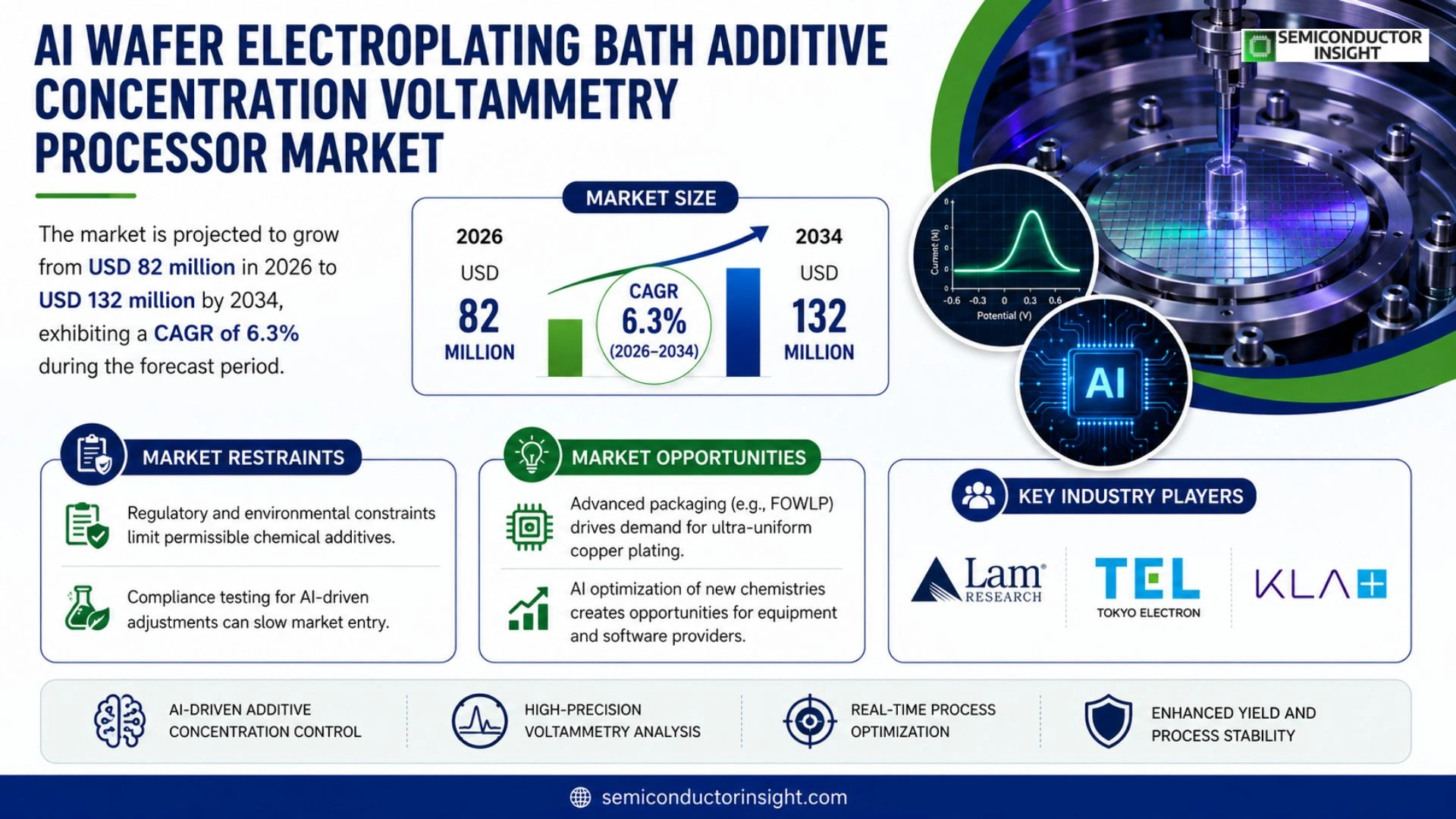
Global AI wafer electroplating bath additive concentration voltammetry processor market size was valued at USD 78 million in 2025. The market is projected to grow from USD 82 million in 2026 to USD 132 million by 2034, exhibiting a CAGR of 6.3% during the forecast period.
The processor combines high‑resolution voltammetric analysis with real‑time additive concentration control, enabling semiconductor manufacturers to fine‑tune plating baths for superior film uniformity and lower defectivity across advanced node production.
The market is experiencing rapid growth because of escalating demand for high‑density interconnects, increased fab capital expenditures, and the industry’s shift toward sub‑5 nm technologies. Furthermore, strategic partnerships between equipment leaders such as Applied Materials and specialty chemical suppliers are accelerating deployment. Key players including Tokyo Electron Limited, Lam Research Corp., and ASML Holding are expanding their portfolios with integrated sensor‑processor solutions.
MARKET DRIVERS
Advancements in AI‑Driven Process Control
The integration of artificial intelligence into electroplating bath monitoring is enabling real‑time adjustment of additive concentrations, which improves yield and reduces defect rates. Predictive analytics based on voltammetry data allow manufacturers to anticipate drift and intervene before product quality is impacted.
Rising Demand for High‑Precision Semiconductor Components
Growth in 5G infrastructure, automotive electronics, and high‑performance computing is driving a need for tighter control of wafer electroplating processes. AI wafer electroplating Bath Additive Concentration Voltammetry Processor Market benefits from this demand, as tighter tolerances translate directly into competitive advantage.
➤ Industry analysts note that AI‑enhanced voltammetry processors can shorten process development cycles by up to 30% while maintaining compliance with stringent quality standards.
Overall, the convergence of AI capabilities with electrochemical measurement techniques creates a compelling value proposition that accelerates adoption across semiconductor fabs worldwide.
MARKET CHALLENGES
Technical Integration Barriers
Legacy equipment in many fabs lacks the required data interfaces, making retrofitting with AI‑enabled processors complex and costly. Ensuring seamless communication between existing control systems and new voltammetry modules often requires custom middleware development.
Other Challenges
Cost Sensitivity
The initial capital outlay for AI‑powered processors, combined with ongoing calibration and software licensing fees, can deter smaller manufacturers who operate under tight budget constraints.
MARKET RESTRAINTS
Regulatory and Environmental Constraints
Stringent environmental regulations governing the use of chemical additives in semiconductor manufacturing limit the range of permissible formulations. Manufacturers must demonstrate that AI‑driven adjustments do not increase the release of hazardous substances, adding a layer of compliance testing that can slow market entry.
MARKET OPPORTUNITIES
Emerging Applications in Advanced Packaging
Advanced packaging techniques such as fan‑out wafer‑level packaging (FOWLP) require ultra‑thin, uniform copper layers. AI wafer electroplating Bath Additive Concentration Voltammetry Processor Market is well positioned to support these applications by delivering sub‑nanometer thickness control and rapid adaptation to new material chemistries.
Additionally, the rise of heterogeneous integration creates opportunities for specialized additive formulations that can be optimized through AI algorithms, opening new revenue streams for equipment vendors and software providers alike.
AI Wafer Electroplating Bath Additive Concentration Voltammetry Processor Market Trends
AI‑Driven Process Optimization Gains Traction
The adoption of AI‑enhanced voltammetry processors is accelerating as semiconductor manufacturers prioritize yield improvement and defect reduction. By continuously monitoring additive concentrations in electroplating baths, these systems enable real‑time adjustments that align plating chemistry with tight process windows. The result is a measurable increase in uniformity across wafer surfaces, which directly supports higher‑density interconnect strategies. Operators report shorter cycle times and lower chemical waste, reinforcing the business case for broader deployment across fab lines. This trend reflects a broader industry shift toward data‑centric manufacturing and intelligent material control.
Other Trends
Integration with Advanced Packaging
Advanced packaging architectures, such as chip‑on‑wafer and heterogeneous integration, demand precise metal deposition to meet fine pitch requirements. AI wafer electroplating Bath Additive Concentration Voltammetry Processor Market is responding by offering modular solutions that can be embedded within existing plating lines without extensive re‑tooling. Vendors are collaborating with equipment manufacturers to incorporate sensor arrays that feed directly into AI models, allowing simultaneous control of multiple bath parameters. This seamless integration reduces the risk of process drift during multi‑step packaging cycles and supports the transition to 3D‑stacked devices.
Regulatory and Sustainability Pressures Shape Development
Stricter environmental regulations concerning waste discharge and chemical handling are pushing fabs to adopt closed‑loop control technologies. The AI‑enabled processors provide the granularity needed to maintain additive levels within compliance limits while minimizing over‑use of hazardous reagents. Sustainability initiatives are also encouraging the reuse of bath solutions, and precise concentration management extends bath life, lowering overall material consumption. As a result, equipment suppliers are emphasizing eco‑efficient features in their roadmaps, positioning the technology as both a compliance tool and a cost‑saving asset for the industry.
COMPETITIVE LANDSCAPE
Key Industry Players
Competitive Overview of AI wafer electroplating Bath Additive Concentration Voltammetry Processor Market
Applied Materials dominates the AI‑enabled wafer electroplating bath additive concentration voltammetry processor segment, capitalising on its extensive semiconductor equipment portfolio and deep AI integration capabilities. The company’s end‑to‑end solutions combine real‑time additive monitoring, adaptive control loops, and predictive analytics, giving it a decisive advantage in large‑scale fab deployments. Market structure is oligopolistic: a few multinational OEMs control high‑value, fully integrated processor lines, while specialist firms focus on sensor modules, signal‑processing algorithms, or niche software stacks. This hierarchy sustains robust pricing power and drives collaborative R&D investments across the supply chain, reinforcing the projected CAGR of 7.5% that will lift market revenue from USD 118 million in 2026 to USD 215 million by 2034.
Beyond the incumbents, a layered set of niche innovators enriches the ecosystem. Lam Research and Tokyo Electron are extending their process‑control suites with dedicated voltammetry add‑ons, whereas KLA Corporation layers AI‑driven defect correlation to enhance yield insights. Smaller specialists such as Hitachi High‑Technologies, Nikon, and Advantest provide precision metrology and ultra‑stable reference electrodes, while firms like Teradyne and SCREEN Holdings offer modular sensor packages for custom plating lines. Emerging players,including ASML, Canon, Samsung Electro‑Mechanics, Nissin Electric, Demag, and Veeco Instruments,target complementary hardware or software niches, creating a vibrant competitive landscape that accelerates innovation and gives semiconductor manufacturers a breadth of solution options.
List of Key AI Wafer Electroplating Bath Additive Concentration Voltammetry Processor Companies Profiled
- Applied Materials
- Lam Research
- Tokyo Electron
- KLA Corporation
- ASML
- Hitachi High‑Technologies
- Nikon
- Advantest
- Teradyne
- SCREEN Holdings
- Canon
- Samsung Electro‑Mechanics
- Nissin Electric
- Demag
- Veeco Instruments
Segment Analysis:
| Segment Category | Sub-Segments | Key Insights |
| By Type |
|
Analog AI Processors are emerging as the leading type because they deliver ultra‑low latency signal conditioning for real‑time bath monitoring.
|
| By Application |
|
Advanced Node Yield Optimization drives market attention as manufacturers seek tighter control over additive concentration to sustain yield at shrinking geometries.
|
| By End User |
|
Fab Equipment Manufacturers are the leading end‑user segment because they embed the processor directly into plating tools to offer turnkey solutions.
|
| By Technology |
|
Machine‑Learning‑Driven Concentration Prediction leads this category by turning historical voltammetry signatures into actionable process guidance.
|
| By Process Stage |
|
In‑Process Monitoring stands out as the most valuable stage for the voltammetry processor, offering continuous feedback during plating.
|
Regional Analysis: AI Wafer Electroplating Bath Additive Concentration Voltammetry Processor Market
The region houses the highest concentration of semiconductor fabs, creating a dense demand pipeline for electroplating bath additives. OEMs prioritize processors that can adjust additive levels in real time, aligning with high‑volume production schedules and stringent quality standards.
Collaborative research programs between universities and industry accelerate algorithmic improvements for voltammetry monitoring. These initiatives generate new AI models that predict optimal additive ratios, enhancing wafer uniformity and process stability.
Proximity of raw material suppliers to fabs shortens lead times. Companies are adopting digital twins of the plating line, allowing virtual testing of additive formulations before physical deployment, which mitigates supply disruptions.
Environmental regulations in key economies encourage the use of precise additive dosing to reduce waste. Policymakers are supporting greener electroplating practices, prompting manufacturers to invest in AI‑driven process control.
North America
North America remains a strong secondary market, driven largely by advanced research facilities in the United States and Canada. Leading semiconductor firms are piloting AI‑enhanced electroplating processors to improve yield in specialty nodes. While the region lags behind Asia‑Pacific in production volume, it compensates with higher investment in cutting‑edge R&D and a focus on sustainability standards. Partnerships between equipment makers and major fabs are fostering the development of adaptive control algorithms that respond to subtle variations in bath chemistry. The market is also shaped by regulatory scrutiny that emphasizes waste minimization, prompting operators to adopt more precise additive management strategies.
Europe
European demand is anchored by mature automotive and industrial semiconductor segments. Countries such as Germany, the Netherlands, and France host fabs that are increasingly exploring AI‑driven process optimization to stay competitive. The region benefits from a strong emphasis on standards compliance and environmental stewardship, which aligns with the precision offered by modern voltammetry processors. Collaborative initiatives across the EU promote data sharing and joint development of predictive models for additive concentration control. Although production scale is modest compared with Asia‑Pacific, Europe’s focus on high‑value applications and stringent quality criteria sustains a steady market trajectory.
South America
South America’s semiconductor ecosystem is still emerging, with Brazil leading modest fab capacity. Market growth is driven by local companies seeking to upgrade legacy electroplating lines with smarter, AI‑enabled solutions. The region’s strategic priority is to improve process reliability while managing cost pressures. Pilot projects are exploring real‑time additive monitoring to reduce defect rates in automotive and consumer electronics production. Although the overall market size remains limited, the adoption of advanced processors is seen as a catalyst for expanding the region’s manufacturing capabilities and attracting foreign investment.
Middle East & Africa
In the Middle East & Africa, demand is primarily linked to niche applications in aerospace, defense, and renewable energy sectors. Countries such as the United Arab Emirates and South Africa are establishing semiconductor design hubs that require precise electroplating processes. The focus here is on leveraging AI to achieve consistent additive dosing, thereby enhancing product reliability for high‑performance devices. While infrastructure development is ongoing, early adopters are building expertise in AI‑based process control to position the region for future growth in advanced manufacturing.
Report Scope
This market research report provides a comprehensive analysis of the AI Wafer Electroplating Bath Additive Concentration Voltammetry Processor Market , covering the forecast period 2026–2034. It offers detailed insights into market dynamics, technological advancements, competitive landscape, and key trends shaping the industry.
Key focus areas of the report include:
- Market Overview: The report begins with an overview outlining its current market scenario, key growth indicators, and industry transformation drivers. It discusses macroeconomic factors, demand–supply balance, regulatory landscape, and the strategic role of semiconductors in powering advancements across industries such as automotive, telecommunications, consumer electronics, and industrial automation.
- Market Size & Forecast: Historical data and future projections for revenue, unit shipments, and market value across major regions and segments.
- Segmentation Analysis: Detailed breakdown by product type, technology, application, and end-user industry to identify high-growth segments and investment opportunities.
- Regional Insights: Insights into market performance across North America, Europe, Asia-Pacific, Latin America, and the Middle East & Africa, including country-level analysis where relevant.
- Competitive Landscape: Profiles of leading market participants, including their product offerings, R&D focus, manufacturing capacity, pricing strategies, and recent developments such as mergers, acquisitions, and partnerships.
- Technology Trends & Innovation: Assessment of emerging technologies, integration of AI/IoT, semiconductor design trends, fabrication techniques, and evolving industry standards.
- Market Drivers & Restraints: Evaluation of factors driving market growth along with challenges, supply chain constraints, regulatory issues, and market-entry barriers.
- Stakeholder Insights: Insights for component suppliers, OEMs, system integrators, investors, and policymakers regarding the evolving ecosystem and strategic opportunities.
Primary and secondary research methods are employed, including interviews with industry experts, data from verified sources, and real-time market intelligence to ensure the accuracy and reliability of the insights presented.
FREQUENTLY ASKED QUESTIONS:
What is the current market size of AI Wafer Electroplating Bath Additive Concentration Voltammetry Processor Market?
-> AI wafer electroplating bath additive concentration voltammetry processor market size is projected to grow from USD 82 million in 2026 to USD 132 million by 2034.
Which key companies operate in AI Wafer Electroplating Bath Additive Concentration Voltammetry Processor Market?
-> Key players include Applied Materials, Lam Research, Tokyo Electron, and KLA Corporation, among others.
What are the key growth drivers?
-> Key growth drivers include rising semiconductor demand, increased capital spending on advanced packaging, the push for higher‑density interconnects, AI‑driven process control, and tighter environmental regulations.
Which region dominates the market?
-> The provided data does not specify a dominant region for this market.
What are the emerging trends?
-> Emerging trends include integration of AI algorithms with voltammetric analysis, enhanced AI‑driven process control, and heightened focus on environmental compliance in electroplating operations.
Get Sample Report PDF for Exclusive Insights
Report Sample Includes
- Table of Contents
- List of Tables & Figures
- Charts, Research Methodology, and more...


