
AI-Specific Analog-to-Digital Converter IP Market Insights
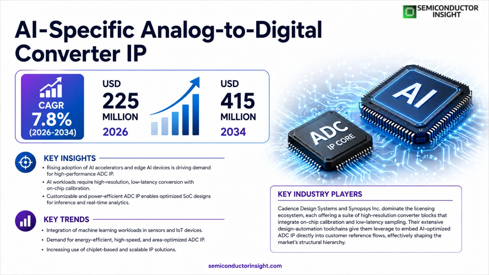
AI-specific analog-to-digital converter IP market size was valued at USD 210 million in 2025. The market will rise from USD 225 million in 2026 to USD 415 million by 2034, reflecting a CAGR of 7.8 % over the forecast horizon.
AI-specific analog-to-digital converter intellectual property comprises reusable design blocks that embed high‑resolution conversion engines optimized for machine‑learning workloads. These cores integrate on‑chip calibration, low‑latency sampling, and power‑efficient architectures tailored for inference accelerators and edge AI processors.
The market gains momentum because semiconductor firms are embedding AI inference directly into sensors and IoT devices, creating demand for converters that can handle heterogeneous data streams without bottlenecking compute units. Moreover, rising capital expenditure on AI‑centric silicon foundries and the emergence of open‑source hardware ecosystems encourage licensing of specialized ADC IP blocks. Companies such as Cadence Design Systems, Synopsys Inc., and imec are expanding their portfolios through strategic collaborations with AI chip designers, further accelerating adoption.
MARKET DRIVERS
AI Workload Intensification Fuels IP Demand
The surge in on‑chip AI inference has forced semiconductor designers to seek converter blocks that can sustain multi‑gigahertz sampling while preserving linearity. AI‑Specific Analog-to-Digital Converter IP delivers precisely calibrated quantization, enabling edge processors to handle vision and speech models without off‑chip bottlenecks. This technical edge shortens time‑to‑market for AI accelerators, a factor that many fabless firms now view as indispensable.
Power‑Efficiency Mandates Shape Architecture Choices
Power budgets for autonomous drones and smart sensors have tightened to under 500 mW per inference engine. Modern ADC IP blocks embed dynamic scaling and clock‑gating mechanisms that trim consumption by 30 %‑40 % compared with legacy designs. Customers prioritize these efficiencies, because lower power translates directly into longer battery life and higher device reliability.
➤ Design houses that integrate AI‑tuned ADC IP report up to a 25 % reduction in silicon area, freeing up die real‑estate for additional neural‑network layers.
Beyond performance, the convergence of AI and mixed‑signal design has created a talent shortage, prompting companies to partner with specialized IP vendors. Such collaborations accelerate design cycles and reduce risk, reinforcing the upward trajectory of the AI‑Specific Analog-to-Digital Converter IP Market.
MARKET CHALLENGES
Integration Complexity Escalates Project Timelines
Embedding high‑precision ADC IP within heterogeneous AI SoCs demands meticulous clock‑domain alignment and meticulous signal‑integrity analysis. Teams that underestimate these intricacies often encounter silicon re‑spins, inflating NRE costs by 15‑20 %. The learning curve for AI‑centric analog design thus remains a noticeable hurdle.
Other Challenges
Supply‑Chain Volatility
The semiconductor substrate market has experienced intermittent shortages, limiting the availability of silicon‑on‑insulator wafers preferred for ultra‑low‑noise converters. This scarcity forces designers to qualify alternative processes, adding verification overhead and extending product rollout windows.
MARKET RESTRAINTS
Cost Sensitivity in Tier‑2 Applications
While flagship AI devices can absorb premium pricing for advanced ADC IP, mid‑range products such as industrial IoT gateways remain price‑conscious. The higher unit cost of AI‑optimized converters, often 1.5‑2× that of generic blocks, dampens adoption in cost‑driven segments, curbing overall market breadth.
MARKET OPPORTUNITIES
Emerging Edge‑AI Platforms Open New Niches
Edge‑AI processors targeting automotive ADAS, wearable health monitors, and smart cameras are scaling from single‑core to multi‑core architectures. Each additional core typically requires a dedicated high‑speed converter to maintain signal fidelity. This architectural shift creates a sizable addressable pool for AI‑Specific Analog-to-Digital Converter IP, especially as OEMs prioritize compact, low‑latency sensor pipelines.
AI-Specific Analog-to-Digital Converter IP Market Trends
AI Inference Embedded Directly in Sensors
The most visible shift in the AI‑Specific Analog-to-Digital Converter IP Market stems from semiconductor manufacturers placing inference engines inside sensor die stacks. This design choice eliminates the need for separate data‑transfer stages, thereby reducing latency that previously hampered real‑time decision making at the edge. Engineers are selecting ADC cores that incorporate on‑chip calibration and ultra‑low‑noise sampling to preserve the fidelity of analog inputs before they enter neural‑network pipelines. The result is a tighter feedback loop between physical measurement and algorithmic response, which is especially valuable for safety‑critical applications such as automotive LIDAR and industrial vision. Companies that can provide IP blocks with deterministic timing and minimal power draw are seeing stronger engagement from OEMs seeking to differentiate their next‑generation products.
Other Trends
Licensing Structures Align With Open‑Source Hardware Momentum
Parallel to the hardware integration trend, licensing strategies are adapting to the rise of collaborative design ecosystems. Traditional royalty‑per‑unit models are giving way to fixed‑fee or subscription arrangements that allow AI chip designers to iterate rapidly without worrying about escalating per‑chip costs. This shift is encouraged by the growing availability of open‑source verification suites, which lower the barrier for integrating third‑party ADC IP into heterogeneous compute fabrics. As a consequence, design houses such as Cadence, Synopsys and imec are packaging their converters with extensive software support, enabling quick prototyping and faster time‑to‑market for AI accelerators destined for edge deployments.
Power‑Optimized Conversion Architectures for AI Workloads
Energy consumption remains a decisive factor for AI‑centric devices operating on limited battery capacity. Recent IP releases emphasize architectural tricks,such as dynamic range scaling and adaptive clock gating,that trim the power envelope of high‑resolution conversion without sacrificing sampling speed. By embedding these efficiencies at the IP level, system architects can meet stringent thermal budgets while still delivering the precision required for quantized deep‑learning inference. This balance is prompting a wave of redesigns in edge AI processors, where the ADC block is no longer an afterthought but a core element of overall power management strategy. Firms that master this integration are positioned to capture a larger share of future AI‑specific silicon investments.
COMPETITIVE LANDSCAPE
Key Industry Players
AI‑Specific ADC IP Landscape 2025‑2034
Cadence Design Systems and Synopsys Inc. dominate the licensing ecosystem, each offering a suite of high‑resolution converter blocks that integrate on‑chip calibration and low‑latency sampling. Their extensive design‑automation toolchains give them leverage to embed AI‑optimized ADC IP directly into customer reference flows, effectively shaping the market’s structural hierarchy. imec’s research‑driven portfolio, while smaller, introduces heterogeneous mixed‑signal architectures that appeal to silicon foundries targeting edge‑AI workloads, thereby creating a secondary tier of specialized providers.
Beyond the frontrunners, a constellation of niche players is expanding the competitive canvas. Texas Instruments and Analog Devices supply differentiated converter families that emphasize power efficiency, attracting automotive and IoT sensor manufacturers. ON Semiconductor and NXP Semiconductors focus on integration‑friendly IP that complements their own MCU and sensor portfolios. Renesas Electronics, GlobalFoundries, and Arm Ltd. contribute design‑blocking services geared toward custom silicon projects, while Marvell Technology, STMicroelectronics, and Infineon Technologies round out the field with application‑specific optimizations for data‑center accelerators and industrial AI edge devices.
List of Key AI‑Specific Analog-to-Digital Converter IP Companies Profiled
- Cadence Design Systems
- Synopsys Inc.
- imec
- Texas Instruments
- Analog Devices
- ON Semiconductor
- NXP Semiconductors
- Renesas Electronics
- GlobalFoundries
- Arm Ltd.
- Marvell Technology
- STMicroelectronics
- Infineon Technologies
Segment Analysis:
| Segment Category | Sub-Segments | Key Insights |
| By Type |
|
Low‑Power ADC IP
|
| By Application |
|
Edge AI Sensors
|
| By End User |
|
Chip Designers
|
| By Integration Level |
|
Embedded within SoC
|
| By Architecture |
|
Sigma‑Delta ADC
|
Regional Analysis: AI-Specific Analog-to-Digital Converter IP Market
North America
Companies are transitioning from one‑time royalty structures to hybrid models that blend upfront fees with usage‑based royalties. This shift reflects the need for customers to scale AI workloads without incurring prohibitive initial costs, while IP owners secure ongoing revenue streams that align with the rise of AI‑centric silicon.
EDA vendors are embedding AI‑Specific ADC IP libraries directly into synthesis and place‑and‑route flows. Designers benefit from early power‑budget estimates, and the tighter integration reduces iteration cycles, a critical advantage in fast‑moving AI product cycles.
Automotive and industrial automation segments are demanding IP with built‑in fault‑tolerance and temperature‑compensated performance. Vendors that embed such attributes into the core IP gain preferential access to OEM programs seeking compliance with safety standards.
The region’s universities continue to produce engineers versed in mixed‑signal AI design, feeding a talent pipeline that sustains both start‑ups and incumbents. This human capital advantage amplifies the speed at which new conversion algorithms are prototyped and commercialized.
Europe
European chip designers are capitalising on the continent’s strong standards‑driven environment, which encourages early alignment with safety and electromagnetic compatibility directives. This regulatory foresight nudges firms toward modular IP that can be certified once and reused across multiple product classes, reducing overhead for AI‑centric applications. Moreover, collaborative research hubs in Germany and France provide a conduit for joint development projects, where academic breakthroughs in low‑power quantisation are rapidly translated into licensable IP blocks. The result is a nuanced ecosystem where design flexibility coexists with rigorous compliance, fostering trust among automotive OEMs and medical‑device manufacturers alike.
Asia‑Pacific
The Asia‑Pacific region is witnessing a surge in AI chipset initiatives, spurred by national programmes that prioritize AI‑ready silicon. While the market is still consolidating, several foundries have begun to offer silicon‑on‑foundry services that bundle AI‑Specific ADC IP with process design kits, effectively lowering entry barriers for emerging fabless firms. At the same time, cost sensitivity drives customers to favour IP that can be tightly tuned for specific power envelopes, prompting vendors to supply extensive parameter libraries. The combination of policy support and pragmatic cost management creates a fertile ground for rapid adoption, especially in consumer electronics and smart‑city deployments.
South America
In South America, the primary catalyst for AI‑Specific ADC IP uptake is the growing emphasis on edge computing in agriculture and logistics. Local manufacturers are integrating AI inference close to sensors to enable real‑time decision making, and the need for high‑resolution, low‑latency conversion is becoming a competitive differentiator. Partnerships between regional universities and multinational IP providers are yielding custom extensions that address tropical temperature variability, ensuring performance stability in harsh environments. These collaborations help bridge the gap between global technology trends and locally relevant applications.
Middle East & Africa
The Middle East & Africa market is still nascent but benefits from substantial investment in smart‑infrastructure projects, such as autonomous transport corridors and renewable‑energy micro‑grids. Stakeholders are looking for IP that can operate reliably under wide voltage swings and high‑temperature conditions typical of desert deployments. Consequently, vendors that can certify their AI‑Specific ADC cores for extended temperature ranges gain early footholds. Additionally, emerging tech incubators in the United Arab Emirates are fostering start‑ups that specialize in AI‑enabled sensor fusion, creating a modest but growing demand for adaptable conversion IP.
Report Scope
This market research report provides a comprehensive analysis of the AI-Specific Analog-to-Digital Converter IP Market , covering the forecast period 2026–2034. It offers detailed insights into market dynamics, technological advancements, competitive landscape, and key trends shaping the industry.
Key focus areas of the report include:
- Market Overview: The report begins with an overview outlining its current market scenario, key growth indicators, and industry transformation drivers. It discusses macroeconomic factors, demand–supply balance, regulatory landscape, and the strategic role of semiconductors in powering advancements across industries such as automotive, telecommunications, consumer electronics, and industrial automation.
- Market Size & Forecast: Historical data and future projections for revenue, unit shipments, and market value across major regions and segments.
- Segmentation Analysis: Detailed breakdown by product type, technology, application, and end-user industry to identify high-growth segments and investment opportunities.
- Regional Insights: Insights into market performance across North America, Europe, Asia-Pacific, Latin America, and the Middle East & Africa, including country-level analysis where relevant.
- Competitive Landscape: Profiles of leading market participants, including their product offerings, R&D focus, manufacturing capacity, pricing strategies, and recent developments such as mergers, acquisitions, and partnerships.
- Technology Trends & Innovation: Assessment of emerging technologies, integration of AI/IoT, semiconductor design trends, fabrication techniques, and evolving industry standards.
- Market Drivers & Restraints: Evaluation of factors driving market growth along with challenges, supply chain constraints, regulatory issues, and market-entry barriers.
- Stakeholder Insights: Insights for component suppliers, OEMs, system integrators, investors, and policymakers regarding the evolving ecosystem and strategic opportunities.
Primary and secondary research methods are employed, including interviews with industry experts, data from verified sources, and real-time market intelligence to ensure the accuracy and reliability of the insights presented.
FREQUENTLY ASKED QUESTIONS:
What is the current market size of AI-Specific Analog-to-Digital Converter IP Market?
-> AI-specific analog-to-digital converter IP market will rise from USD 225 million in 2026 to USD 415 million by 2034, reflecting a CAGR of 7.8 %
Which key companies operate in AI-Specific Analog-to-Digital Converter IP Market?
-> Key players include Cadence Design Systems, Synopsys Inc., and imec, among others.
What are the key growth drivers?
-> Key growth drivers include embedding AI inference into sensors and IoT devices, rising demand for high‑resolution ADC IP, increasing capital expenditure on AI‑centric silicon foundries, and the emergence of open‑source hardware ecosystems.
Which region dominates the market?
-> The reference does not specify a single dominant region; the market is global with activity across major semiconductor hubs.
What are the emerging trends?
-> Emerging trends include open‑source hardware ecosystems, AI‑centric silicon foundry investments, and strategic collaborations between IP vendors and AI chip designers.

Get Sample Report PDF for Exclusive Insights
Report Sample Includes
- Table of Contents
- List of Tables & Figures
- Charts, Research Methodology, and more...
 Download Sample Report PDF




