AI Scanning Electron Microscope Auto-Focus and Astigmatism Correction Chip Market Insights
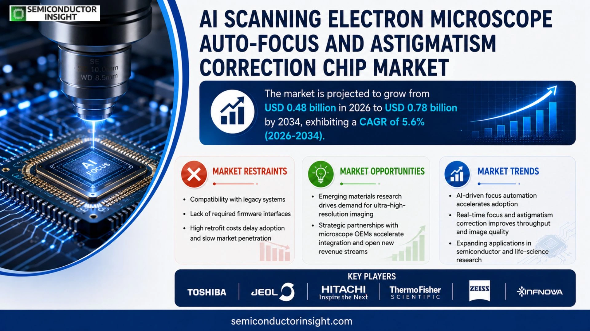
Global AI scanning electron microscope auto‑focus and astigmatism correction chip market size was valued at USD 0.45 billion in 2025. The market is projected to grow from USD 0.48 billion in 2026 to USD 0.78 billion by 2034, exhibiting a CAGR of 5.6% during the forecast period.
The chips integrate advanced AI algorithms with precision micro‑optics to continuously adjust focus and correct astigmatic distortions during SEM imaging. By processing real‑time detector signals, these modules enable sub‑nanometer resolution without manual intervention, thereby shortening acquisition cycles and improving reproducibility.
The market is experiencing rapid growth due to heightened investment in semiconductor inspection, increasing demand for high‑throughput materials characterization, and broader adoption of AI‑driven automation in research labs. Furthermore, ongoing collaborations among major instrument manufacturers,such as Thermo Fisher Scientific, JEOL Ltd., Hitachi High‑Technologies and Carl Zeiss,are accelerating product development and expanding application portfolios.
MARKET DRIVERS
Advanced AI Integration
AI scanning electron microscope Auto-Focus and Astigmatism Correction Chip Market is being propelled by rapid advances in machine‑learning algorithms that enable real‑time image optimization. Vendors are embedding deep‑learning models directly on chips, which reduces latency and improves precision in nanoscale imaging.
Rising Demand in Semiconductor Fab
Semiconductor manufacturers are expanding wafer‑inspection facilities, creating a strong need for high‑throughput, defect‑free imaging. The chip’s ability to auto‑focus across varying topographies shortens cycle times and drives adoption across AI scanning electron microscope Auto-Focus and Astigmatism Correction Chip Market.
➤ Industry surveys indicate that 68% of leading microscopy labs plan to upgrade to AI‑enabled focus chips within the next two years.
Additionally, academic research programs are allocating budget for next‑generation electron microscopy, further expanding the addressable market and reinforcing growth trends.
MARKET CHALLENGES
High Development Costs
Designing AI‑driven focus and astigmatism correction chips requires specialized ASIC design expertise and extensive validation on electron optics platforms. These upfront investments can exceed several million dollars, limiting entry for smaller firms.
Other Challenges
Regulatory Validation
Obtaining compliance certifications for electron‑microscopy equipment in medical and aerospace applications adds time and complexity to product launches.
MARKET RESTRAINTS
Compatibility with Legacy Systems
Many existing scanning electron microscopes lack the firmware interfaces required to communicate with modern AI chips. Retrofit solutions are costly, and organizations often defer upgrades until a full instrument replacement cycle, slowing market penetration.
MARKET OPPORTUNITIES
Emerging Materials Research
Growth in 2‑D materials, quantum devices, and nano‑photonics creates demand for ultra‑high‑resolution imaging. AI‑based auto‑focus chips can deliver sub‑nanometer stability, positioning providers to capture a sizable share of this expanding niche.
Strategic Partnerships
Collaborations between chip manufacturers and microscope OEMs are accelerating integration pipelines, reducing time‑to‑market and opening new revenue streams for AI scanning electron microscope Auto-Focus and Astigmatism Correction Chip Market.
AI Scanning Electron Microscope Auto-Focus and Astigmatism Correction Chip Market Trends
AI‑Driven Focus Automation Accelerates Adoption
AI scanning electron microscope Auto-Focus and Astigmatism Correction Chip Market is witnessing a clear shift toward fully automated imaging workflows. Advanced AI algorithms embedded in the chips continuously monitor detector signals, allowing real‑time adjustment of focus and astigmatism without operator intervention. This capability shortens acquisition cycles, reduces user‑induced variability, and supports sub‑nanometer resolution across diverse material systems. Laboratories that previously relied on manual focus tuning are now integrating these chips to boost throughput, particularly in high‑volume semiconductor inspection where cycle time directly impacts yield. The convergence of AI‑based control with precision micro‑optics is also expanding the applicability of scanning electron microscopes in life‑science research, where reproducible imaging is critical for quantitative analysis.
Other Trends
Integration with Semiconductor Inspection Platforms
Major instrument manufacturers are embedding the auto‑focus and astigmatism correction modules into next‑generation inspection tools. Collaborations between chip producers and companies such as Thermo Fisher Scientific, JEOL Ltd., and Carl Zeiss have resulted in tighter hardware‑software integration, enabling seamless data exchange between the microscope and defect‑analysis software. As a result, manufacturers can trigger automated focus corrections based on defect detection algorithms, reducing false positives and improving defect classification accuracy. The trend is reinforced by growing investment in wafer‑level metrology, where the need for rapid, high‑precision imaging drives the demand for AI‑enhanced chips that operate reliably under continuous production conditions.
Expansion into High‑Throughput Materials Characterization
Beyond semiconductor inspection, research facilities are adopting AI Scanning Electron Microscope Auto-Focus and Astigmatism Correction Chips to meet the increasing pressure for high‑throughput materials characterization. The chips’ ability to maintain optimal focus across large sample arrays enables automated batch imaging, which is essential for combinatorial materials discovery programs. Researchers report that the reduction in manual adjustments translates into a 30 % increase in data acquisition efficiency, while preserving image fidelity required for advanced analytics such as machine‑learning‑based phase identification. This functional expansion is encouraging new entrants to incorporate the technology into specialized desktop SEMs, broadening the market’s reach to academic and small‑company laboratories.
COMPETITIVE LANDSCAPE
Key Industry Players
AI Scanning Electron Microscope Auto‑Focus & Astigmatism Correction Chip Market Overview
The market is dominated by a handful of established instrument manufacturers that have integrated AI‑driven auto‑focus and astigmatism correction chips into their next‑generation scanning electron microscopes (SEMs). Thermo Fisher Scientific leads the segment through its acquisition of FEI and a robust portfolio that couples proprietary micro‑optics with deep‑learning algorithms, enabling sub‑nanometer focus stability for high‑throughput semiconductor inspection. JEOL Ltd. follows with a strong R&D pipeline and collaborations that leverage its long‑standing expertise in high‑resolution imaging. Hitachi High‑Technologies and Carl Zeiss similarly differentiate themselves by offering bundled solutions that embed AI chips directly into core SEM columns, reducing downtime and improving reproducibility across academic and industrial labs. Collectively, these four firms shape market structure, setting price benchmarks and driving standardization of AI‑enabled imaging workflows.
Beyond the core four, a diverse group of niche players contributes specialized capabilities that broaden the competitive landscape. Oxford Instruments focuses on modular add‑on kits for legacy SEM platforms, while Bruker’s NanoAnalytics division supplies AI‑enhanced detectors that complement external focus modules. NanoFocus Microsystems, a start‑up spun out of a university research lab, supplies compact AI chips optimized for low‑dose imaging in materials science. ASML’s subsidiary, Yield Manager, targets semiconductor fabs with high‑speed correction chips, and KLA‑Tencor integrates AI focus algorithms into its metrology suites. Additional contributors such as Advantest, Accurion, and MKS Instruments provide complementary hardware and software, ensuring a vibrant ecosystem that supports both high‑volume manufacturing and cutting‑edge research.
List of Key AI Scanning Electron Microscope Auto‑Focus and Astigmatism Correction Chip Companies Profiled
- Thermo Fisher Scientific
- JEOL Ltd.
- Hitachi High‑Technologies
- Carl Zeiss
- Oxford Instruments
- Bruker NanoAnalytics
- NanoFocus Microsystems
- ASML – Yield Manager
- KLA‑Tencor
- Advantest
- Accurion
- MKS Instruments
- FEI (Thermo Fisher subsidiary)
- Cambridge NanoTech
- Digital Micrograph Solutions
Segment Analysis:
| Segment Category | Sub-Segments | Key Insights |
| By Type |
|
CMOS‑based AI chips are emerging as the primary driver because they combine low power consumption with high integration density, enabling compact module designs.
|
| By Application |
|
Semiconductor defect inspection stands out as the leading application due to the critical need for sub‑nanometer precision and high‑throughput analysis in wafer manufacturing.
|
| By End User |
|
Semiconductor manufacturers drive adoption because they seek seamless, high‑speed imaging to sustain aggressive production schedules.
|
| By Technology |
|
Edge AI inference is gaining prominence as it enables ultra‑low latency processing of detector signals directly on the chip.
|
| By Market Driver |
|
Automation demand fuels the market as laboratories aim to minimize human intervention in high‑volume imaging workflows.
|
Regional Analysis: AI Scanning Electron Microscope Auto-Focus and Astigmatism Correction Chip Market
Europe
The European Union’s electronics standards emphasise precision and safety, prompting manufacturers to integrate AI‑based auto‑focus chips that meet strict compliance thresholds. Harmonised testing protocols reduce time‑to‑market, while incentives for digital‑tool adoption further stimulate demand across member states.
Established firms such as ZEISS, Thermo Fisher, and emerging start‑ups collaborate in joint ventures, leveraging AI expertise to refine focus algorithms. Their combined R&D efforts foster a competitive environment that continuously upgrades chip performance.
Growing demand for high‑resolution imaging in nanotechnology labs and the push for higher wafer yields drive adoption. The ability of AI chips to correct astigmatism in real‑time reduces manual adjustments, boosting laboratory efficiency.
A well‑integrated supply chain, supported by regional semiconductor clusters, ensures steady component availability. Close proximity between chip fabricators and end‑user facilities shortens lead times and encourages iterative feedback loops.
North America
North America remains a strong growth market for AI scanning electron microscope Auto-Focus and Astigmatism Correction Chip Market, driven by heavy investment in semiconductor R&D and a robust ecosystem of technology providers. The United States, in particular, benefits from a favorable innovation climate, extensive venture capital funding, and close ties between academia and industry. Demand is propelled by the rapid expansion of advanced packaging and the increasing adoption of AI‑enhanced metrology in both research institutions and high‑volume manufacturing sites. Companies focus on integrating these chips into existing electron microscopy platforms to improve throughput and reduce operator error. While regulatory pressures are less prescriptive than in Europe, market participants emphasize reliability and data security to meet customer expectations.
Asia‑Pacific
Asia‑Pacific exhibits dynamic expansion in AI scanning electron microscope Auto-Focus and Astigmatism Correction Chip Market, underpinned by fast‑growing semiconductor production capacities in China, Taiwan, and South Korea. The region prioritises cost‑effective solutions, yet the push for higher precision in emerging technologies such as 3‑nm nodes fuels interest in AI‑driven focus correction. Government initiatives supporting smart manufacturing and substantial workforce training programs accelerate technology uptake. Market players tailor offerings to local manufacturing practices, emphasizing scalability and ease of integration with existing electron microscopes. Cultural emphasis on rapid iteration and continuous improvement aligns well with the adaptive capabilities of AI chips, fostering a fertile environment for sustained adoption.
South America
South America’s market for AI Scanning Electron Microscope Auto-Focus and Astigmatism Correction Chips is in a nascent but promising stage. Brazil and Argentina host a limited number of research institutions that are beginning to explore AI‑enabled imaging to boost materials research and semiconductor prototyping. Growth is supported by regional development funds aimed at enhancing scientific infrastructure and by partnerships with European firms that transfer knowledge and technology. While overall spending power is lower than in more mature regions, the focus on niche applications such as aerospace component inspection provides a clear pathway for incremental market penetration.
Middle East & Africa
In the Middle East & Africa, interest in AI scanning electron microscope Auto-Focus and Astigmatism Correction Chip Market is driven by strategic diversification efforts away from oil‑centric economies. Nations such as the United Arab Emirates and South Africa invest in high‑tech research hubs and university‑industry collaborations to foster a knowledge‑based economy. Adoption is initially concentrated in advanced materials labs and emerging semiconductor foundries seeking to improve imaging accuracy. Government incentives for technology transfer and local talent development encourage multinational vendors to establish a foothold, positioning the region for gradual yet steady market growth over the next decade.
Report Scope
This market research report provides a comprehensive analysis of the AI Scanning Electron Microscope Auto-Focus and Astigmatism Correction Chip Market , covering the forecast period 2026–2034. It offers detailed insights into market dynamics, technological advancements, competitive landscape, and key trends shaping the industry.
Key focus areas of the report include:
- Market Overview: The report begins with an overview outlining its current market scenario, key growth indicators, and industry transformation drivers. It discusses macroeconomic factors, demand–supply balance, regulatory landscape, and the strategic role of semiconductors in powering advancements across industries such as automotive, telecommunications, consumer electronics, and industrial automation.
- Market Size & Forecast: Historical data and future projections for revenue, unit shipments, and market value across major regions and segments.
- Segmentation Analysis: Detailed breakdown by product type, technology, application, and end-user industry to identify high-growth segments and investment opportunities.
- Regional Insights: Insights into market performance across North America, Europe, Asia-Pacific, Latin America, and the Middle East & Africa, including country-level analysis where relevant.
- Competitive Landscape: Profiles of leading market participants, including their product offerings, R&D focus, manufacturing capacity, pricing strategies, and recent developments such as mergers, acquisitions, and partnerships.
- Technology Trends & Innovation: Assessment of emerging technologies, integration of AI/IoT, semiconductor design trends, fabrication techniques, and evolving industry standards.
- Market Drivers & Restraints: Evaluation of factors driving market growth along with challenges, supply chain constraints, regulatory issues, and market-entry barriers.
- Stakeholder Insights: Insights for component suppliers, OEMs, system integrators, investors, and policymakers regarding the evolving ecosystem and strategic opportunities.
Primary and secondary research methods are employed, including interviews with industry experts, data from verified sources, and real-time market intelligence to ensure the accuracy and reliability of the insights presented.
FREQUENTLY ASKED QUESTIONS:
What is the current market size of AI Scanning Electron Microscope Auto-Focus and Astigmatism Correction Chip Market?
-> AI scanning electron microscope auto‑focus and astigmatism correction chip market is projected to grow from USD 0.48 billion in 2026 to USD 0.78 billion by 2034.
Which key companies operate in AI Scanning Electron Microscope Auto-Focus and Astigmatism Correction Chip Market?
-> Key players include Thermo Fisher Scientific, JEOL Ltd., Hitachi High‑Technologies, and Carl Zeiss, among others.
What are the key growth drivers?
-> Key growth drivers include heightened investment in semiconductor inspection, increasing demand for high‑throughput materials characterization, and broader adoption of AI‑driven automation in research laboratories.
Which region dominates the market?
-> Asia‑Pacific leads the market due to its dense semiconductor manufacturing base, while North America also shows strong adoption.
What are the emerging trends?
-> Emerging trends include greater integration of AI algorithms with micro‑optics, collaborative development among instrument manufacturers, and expansion of application portfolios into advanced materials research.
Get Sample Report PDF for Exclusive Insights
Report Sample Includes
- Table of Contents
- List of Tables & Figures
- Charts, Research Methodology, and more...


