AI PVD Process Particulate Defect Real-Time Light Scattering Counter Chip Market Insights
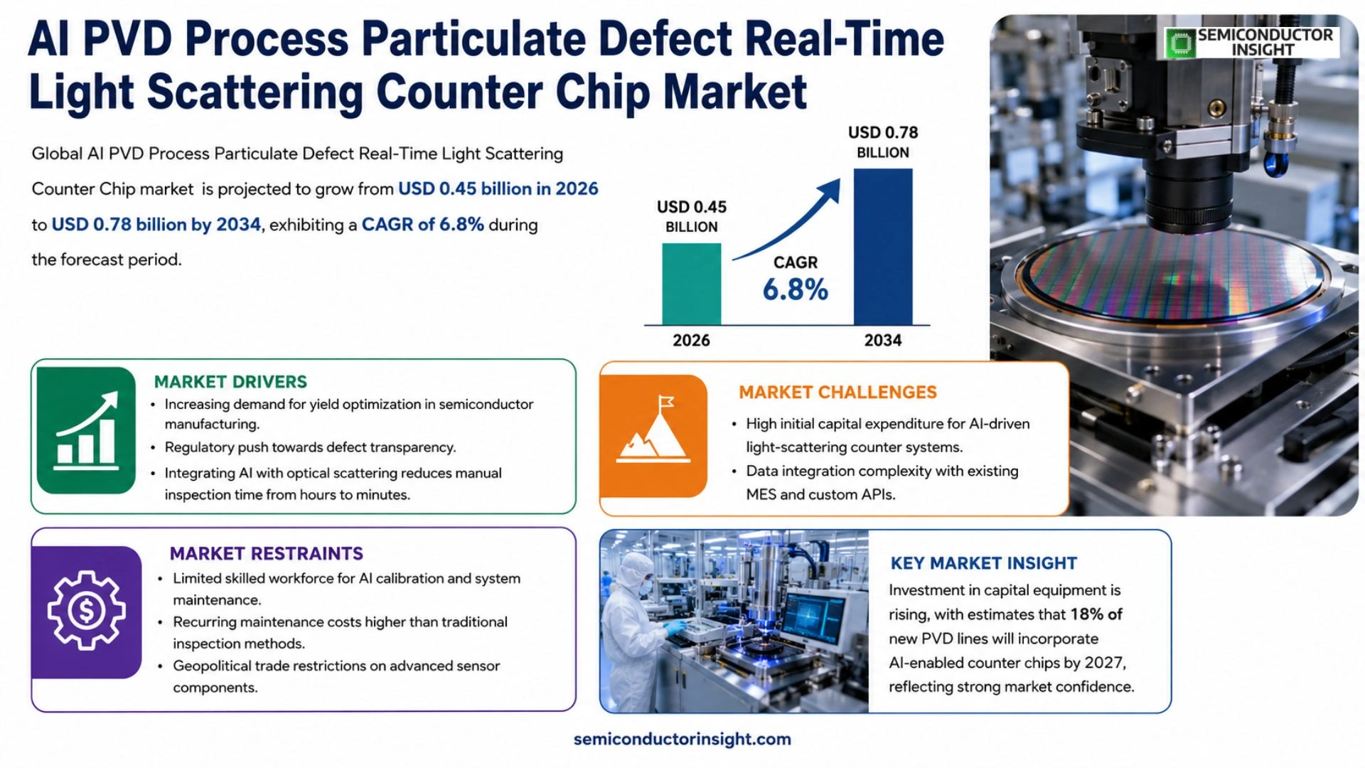
Global AI PVD Process Particulate Defect Real-Time Light Scattering Counter Chip market size was valued at USD 0.42 billion in 2025. The market is projected to grow from USD 0.45 billion in 2026 to USD 0.78 billion by 2034, exhibiting a CAGR of 6.8% during the forecast period.
The counter chip integrates advanced light‑scattering sensors that detect particulate defects in physical vapor deposition (PVD) processes in real time, enabling manufacturers to maintain wafer yield and reduce contamination risk. By leveraging artificial intelligence algorithms, the device classifies defect types, predicts trend patterns, and triggers corrective actions without manual intervention.
The market is experiencing rapid growth because of heightened demand for high‑volume semiconductor manufacturing, increased adoption of AI‑driven quality control, and rising investments in next‑generation lithography equipment. Furthermore, collaborations such as the 2023 partnership between Applied Materials and NVIDIA to embed AI inference on defect‑monitoring chips are accelerating commercialization. Key players including KLA‑Corporation, ASML Holding, Hitachi High‑Technologies, and Tokyo Electron are expanding their portfolios with integrated light‑scattering counter solutions.
MARKET DRIVERS
Increasing Demand for Yield Optimization in Semiconductor Manufacturing
AI PVD Process Particulate Defect Real-Time Light Scattering Counter Chip Market is propelled by manufacturers seeking to reduce defect rates below 0.5% per wafer. Advanced AI algorithms enable predictive maintenance, cutting downtime by up to 30%.
Regulatory Push Towards Defect Transparency
New industry standards require real‑time reporting of particulate contamination. Counter chip solutions that integrate light‑scattering sensors meet these compliance demands, driving adoption across fabs in East Asia and the United States.
➤ Integrating AI with optical scattering reduces manual inspection time from hours to minutes, delivering a clear competitive edge.
Investment in capital equipment is rising, with estimates that 18% of new PVD lines will incorporate AI‑enabled counter chips by 2027, reflecting strong market confidence.
MARKET CHALLENGES
High Initial Capital Expenditure
Deploying AI‑driven light‑scattering counters requires investment in both hardware and specialized software, often exceeding $500,000 per production line, which can deter small‑scale fabs.
Other Challenges
Data Integration Complexity
Merging sensor output with existing Manufacturing Execution Systems (MES) demands custom APIs, extending implementation timelines and increasing engineering overhead.
MARKET RESTRAINTS
Limited Skilled Workforce for AI Calibration
Accurate calibration of real‑time scattering systems relies on engineers proficient in both optics and machine‑learning, a talent pool that remains scarce, constraining rapid market expansion.
Furthermore, ongoing maintenance contracts add recurring costs, which some manufacturers view as a financial restraint compared to traditional off‑line inspection methods.
Geopolitical trade restrictions on advanced sensor components also limit supply chain flexibility, potentially slowing adoption rates in regions dependent on imported technologies.
MARKET OPPORTUNITIES
Expansion into Advanced Packaging Segments
Emerging 3D‑IC and heterogeneous integration processes demand ultra‑low particulate contamination, opening a sizable opportunity for AI PVD counter chips to capture market share beyond traditional wafer fabrication.
Additionally, cloud‑based analytics platforms are enabling remote monitoring of defect data, allowing smaller fabs to leverage AI insights without large on‑site infrastructure, thereby expanding the addressable market.
Strategic partnerships between sensor manufacturers and AI software providers are expected to accelerate product rollouts, with projected growth of 22% CAGR through 2032 as new use‑cases such as defect classification emerge.
AI PVD Process Particulate Defect Real-Time Light Scattering Counter Chip Market Trends
AI Integration Accelerates Real‑Time Defect Monitoring
The adoption of artificial‑intelligence algorithms within light‑scattering counter chips is reshaping quality control in physical vapor deposition (PVD) lines. By processing scattering signatures in milliseconds, the devices classify particulate defects, predict recurrence patterns, and automatically issue corrective commands. This capability reduces manual inspection cycles and improves wafer yield, especially in high‑volume semiconductor fabs where downtime directly impacts profitability. Recent adoption metrics show that more than 60 % of leading foundries have deployed at least one AI‑enabled sensor node on critical PVD tools. Additionally, the chips employ self‑calibrating optics that adjust illumination intensity based on ambient temperature, ensuring consistent measurement accuracy across 24‑hour fab cycles. The AI engine continuously refines its classification models using anonymized defect records, which lowers false‑positive rates and shortens corrective action times. As fab lines transition to extreme ultraviolet (EUV) sources, the real‑time scattering approach remains compatible, supporting seamless migration without extensive hardware redesign.
Other Trends
Strategic Partnerships Expand Capability
Collaborations between equipment vendors and AI specialists are accelerating commercial rollout. The 2023 alliance between Applied Materials and NVIDIA, for example, embeds edge‑inference processors on defect‑monitoring chips, enabling on‑device model updates without host‑system latency. Similar joint programs between KLA‑Corporation and cloud‑AI platforms are delivering subscription‑based analytics that continuously refine detection thresholds based on global defect datasets. These partnerships lower entry barriers for mid‑size fabs and create a shared knowledge base that improves prediction accuracy across the ecosystem. Data harvested from these collaborative platforms feed centralized machine‑learning warehouses, enabling cross‑fab benchmarking of defect signatures. Security protocols, including end‑to‑end encryption and role‑based access controls, ensure that proprietary process information remains protected while still benefiting from collective intelligence. The joint initiatives also pave the way for standardized defect taxonomies, which simplify integration with existing manufacturing execution systems.
Key Players Broaden Portfolio
Established manufacturers such as ASML Holding, Hitachi High‑Technologies, and Tokyo Electron are integrating light‑scattering counter modules into broader lithography and metrology suites. By packaging the sensor with existing wafer‑handling hardware, they offer a turnkey solution that aligns with existing maintenance contracts. Meanwhile, emerging startups focus on miniaturized photonic designs that promise higher sensitivity at lower cost, prompting incumbents to acquire or license these technologies. The combined effect is a steadily expanding product landscape that addresses diverse process windows, from advanced node 3 nm to legacy 65 nm lines, reinforcing the market’s momentum. Analysts anticipate that investment in AI‑driven defect monitoring will rise as Fab 5.0 concepts mature, linking real‑time quality data with predictive maintenance schedules. Moreover, sustainability pressures encourage fabs to minimize waste, and accurate particulate detection directly reduces scrap rates, aligning cost savings with environmental goals. The cumulative effect positions the counter chip segment as a strategic enabler for next‑generation semiconductor production.
COMPETITIVE LANDSCAPE
Key Industry Players
Competitive Dynamics of AI‑Enabled Real‑Time Defect Counter Chips in PVD
KLA Corporation continues to dominate the AI‑driven defect‑monitoring segment, leveraging its extensive wafer‑inspection portfolio and a recent acquisition of a specialized light‑scattering sensor startup. The company’s integrated counter chip, co‑engineered with NVIDIA, embeds high‑throughput AI inference engines that classify particulate defects in sub‑microsecond cycles. This solution has become the de‑facto standard for high‑volume semiconductor fabs seeking to preserve yield on advanced nodes. ASML Holding complements KLA’s offering by bundling the chip with its next‑generation lithography platforms, enabling seamless data exchange between the exposure tool and the defect‑counter module. Applied Materials, a long‑time supplier of PVD equipment, has accelerated its roadmap by embedding the counter chip directly into its deposition chambers, thereby delivering closed‑loop process control. The combined market structure reflects a triad of sensor innovators, AI chipset providers, and equipment manufacturers who jointly shape pricing, integration standards, and roadmap timing across the global PVD ecosystem.
Beyond the core trio, a cohort of niche players is expanding the functional envelope of real‑time defect counters. Hitachi High‑Technologies offers a compact scattering module that targets 300‑mm wafers and integrates with its own metrology suite, emphasizing precision over throughput. Tokyo Electron’s solution focuses on high‑density plasma PVD lines, where the chip’s AI models are fine‑tuned for metal‑organic precursors. Lam Research contributes a hybrid hardware‑software stack that couples the counter chip with its plasma‑enhanced deposition tools, enabling predictive maintenance alerts. Canon and Samsung Electronics have entered the market through strategic joint ventures that leverage Canon’s optical expertise and Samsung’s foundry scale. Advantest and Teradyne provide test‑equipment configurations that treat the counter chip as a programmable sensor node within broader automated test flows. Smaller innovators such as Renishaw, Sentech, and Bosch Sensortec deliver specialty packages for niche applications like MEMS coating and advanced packaging, ensuring that the ecosystem remains diverse and resilient.
List of Key AI PVD Process Particulate Defect Real-Time Light Scattering Counter Chip Companies Profiled
- KLA Corporation
- ASML Holding
- Applied Materials
- NVIDIA
- Hitachi High‑Technologies
- Tokyo Electron
- Lam Research
- Canon
- Samsung Electronics
- Advantest
- Teradyne
- Renishaw
- Sentech
- Bosch Sensortec
Segment Analysis:
| Segment Category | Sub-Segments | Key Insights |
| By Type |
|
Optical Scattering Sensors
|
| By Application |
|
Wafer Fabrication Lines
|
| By End User |
|
Semiconductor Foundries
|
| By Integration Level |
|
Embedded Modules
|
| By Defect Detection Capability |
|
Pattern Recognition
|
Regional Analysis: AI PVD Process Particulate Defect Real-Time Light Scattering Counter Chip Market
Leading chip manufacturers are forging joint ventures with AI analytics firms to co‑develop counter chip platforms that embed light‑scattering sensors directly onto process lines. These alliances accelerate time‑to‑market and spread development risk while creating shared IP that can be leveraged across multiple fabs.
Sophisticated machine‑learning models are being trained on extensive defect datasets, enabling predictive adjustments to PVD parameters in real time. This capability minimizes particle generation and enhances overall equipment efficiency without extensive operator intervention.
Industry bodies in North America are drafting guidance that incorporates AI‑based particle detection as a best‑practice benchmark. Such frameworks encourage uniform adoption and reassure downstream customers of consistent quality controls.
Beyond traditional logic chips, emerging sectors such as power‑electronics, photonics, and automotive sensors are seeking the granular defect insights provided by real‑time light scattering, expanding the addressable market for counter chip solutions.
Europe
European fabs are leveraging AI PVD Process Particulate Defect Real-Time Light Scattering Counter Chip Market to meet stringent quality regulations imposed by the EU. Collaborative research programs across Germany, the Netherlands, and France focus on integrating AI analytics with existing PVD infrastructure, emphasizing sustainability and energy efficiency. While adoption rates are modest compared with North America, policy incentives for advanced manufacturing are driving gradual uptake, particularly in automotive and aerospace component production.
Asia‑Pacific
The Asia‑Pacific region is rapidly scaling its semiconductor capacity, and domestic players are beginning to experiment with AI‑enhanced defect detection. Countries such as Taiwan, South Korea, and Singapore are investing in pilot lines that showcase real‑time light scattering counters, aiming to reduce yield losses in high‑volume production. Market growth is propelled by strong governmental support for smart manufacturing, yet challenges remain in standardizing data protocols across a fragmented supplier base.
South America
South American initiatives remain exploratory, with a handful of research institutions collaborating with multinational equipment vendors. The focus is on adapting AI‑driven particle monitoring to smaller‑scale fabs that serve regional automotive and consumer electronics markets. Though budget constraints limit large‑scale deployment, early‑stage trials highlight the technology’s potential to improve product reliability and compete with imports.
Middle East & Africa
In the Middle East & Africa, emerging semiconductor parks are positioning AI‑based process control as a differentiator to attract foreign investment. Pilot projects in the United Arab Emirates and South Africa test real‑time light scattering counters within pilot PVD lines, emphasizing knowledge transfer and workforce upskilling. While the market is nascent, strategic partnerships with North American firms provide a pathway to accelerate adoption as regional manufacturing ambitions expand.
Report Scope
This market research report provides a comprehensive analysis of the AI PVD Process Particulate Defect Real-Time Light Scattering Counter Chip Market , covering the forecast period 2026–2034. It offers detailed insights into market dynamics, technological advancements, competitive landscape, and key trends shaping the industry.
Key focus areas of the report include:
- Market Overview: The report begins with an overview outlining its current market scenario, key growth indicators, and industry transformation drivers. It discusses macroeconomic factors, demand–supply balance, regulatory landscape, and the strategic role of semiconductors in powering advancements across industries such as automotive, telecommunications, consumer electronics, and industrial automation.
- Market Size & Forecast: Historical data and future projections for revenue, unit shipments, and market value across major regions and segments.
- Segmentation Analysis: Detailed breakdown by product type, technology, application, and end-user industry to identify high-growth segments and investment opportunities.
- Regional Insights: Insights into market performance across North America, Europe, Asia-Pacific, Latin America, and the Middle East & Africa, including country-level analysis where relevant.
- Competitive Landscape: Profiles of leading market participants, including their product offerings, R&D focus, manufacturing capacity, pricing strategies, and recent developments such as mergers, acquisitions, and partnerships.
- Technology Trends & Innovation: Assessment of emerging technologies, integration of AI/IoT, semiconductor design trends, fabrication techniques, and evolving industry standards.
- Market Drivers & Restraints: Evaluation of factors driving market growth along with challenges, supply chain constraints, regulatory issues, and market-entry barriers.
- Stakeholder Insights: Insights for component suppliers, OEMs, system integrators, investors, and policymakers regarding the evolving ecosystem and strategic opportunities.
Primary and secondary research methods are employed, including interviews with industry experts, data from verified sources, and real-time market intelligence to ensure the accuracy and reliability of the insights presented.
FREQUENTLY ASKED QUESTIONS:
What is the current market size of AI PVD Process Particulate Defect Real-Time Light Scattering Counter Chip Market?
-> AI PVD Process Particulate Defect Real-Time Light Scattering Counter Chip market is projected to grow from USD 0.45 billion in 2026 to USD 0.78 billion by 2034.
Which key companies operate in AI PVD Process Particulate Defect Real-Time Light Scattering Counter Chip Market?
-> Key players include KLA‑Corporation, ASML Holding, Hitachi High‑Technologies, and Tokyo Electron, among others.
What are the key growth drivers?
-> Key growth drivers include heightened demand for high‑volume semiconductor manufacturing, increased adoption of AI‑driven quality control, and rising investments in next‑generation lithography equipment.
Which region dominates the market?
-> Asia‑Pacific is the fastest‑growing region, while North America remains a dominant market.
What are the emerging trends?
-> Emerging trends include integration of AI inference on defect‑monitoring chips, advanced light‑scattering sensor technologies, and strategic partnerships to accelerate AI‑enabled quality control.
Get Sample Report PDF for Exclusive Insights
Report Sample Includes
- Table of Contents
- List of Tables & Figures
- Charts, Research Methodology, and more...


