Key Statistics
Key Takeaways
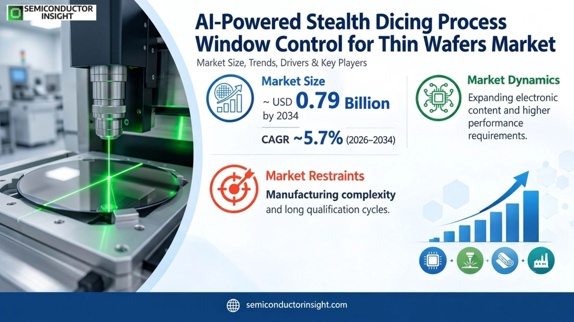
- The AI-Powered Stealth Dicing Process Window Control for Thin Wafers Market was valued at USD 0.46 billion in the 2025 base year and is projected to reach USD 0.79 billion by 2034, expanding at a 5.7% CAGR during 2026–2034.
- Laser-Based Stealth Dicing is a leading product grouping because customers value qualified performance, integration readiness, and lifecycle support.
- Logic Chip Manufacturing is a major demand centre, while adjacent uses broaden the addressable opportunity.
- Asia Pacific leads the regional market through concentrated manufacturing, customers, and technology investment.
- Reliability, qualification, process control, and total ownership economics shape competition.
AI-Powered Stealth Dicing Process Window Control for Thin Wafers Market Overview
AI-Powered Stealth Dicing Process Window Control for Thin Wafers Market was valued at USD 0.46 billion in 2025 and is projected to reach USD 0.79 billion by 2034, growing at a CAGR of 5.7% during 2026–2034. Asia Pacific held the largest regional position in 2025, supported by concentrated manufacturing, downstream electronics production and established component su pply networks.
AI-powered stealth dicing process-window control combines laser or blade dicing with sensor data, machine-learning models, and closed-loop recipe adjustment. The system monitors wafer thickness, focus, power, vibration, edge condition, and defect signals to reduce chipping and improve cut consistency in thin substrates. The analysis also considers qualification requirements, supplier capability, regional purchasing conditions, technology substitution, operating economics, implementation risk, customer procurement cycles, lifecycle support, regulatory context, and evidence required for sustained commercial adoption through the forecast period.
The 2026 estimated year reflects pressure to thin wafers below 150 micrometres while protecting die strength, yield, and cycle time. Logic, memory, power, image-sensor, MEMS, and advanced-packaging lines can benefit when process variability makes fixed dicing recipes unreliable. The analysis also considers qualification requirements, supplier capability, regional purchasing conditions, technology substitution, operating economics, implementation risk, customer procurement cycles, lifecycle support, regulatory context, and evidence required for sustained commercial adoption through the forecast period.
The market is an emerging equipment-and-software segment. Suppliers compete through sensing, algorithms, motion control, laser sources, inspection, recipe libraries, integration with factory systems, and the ability to prove repeatable yield improvement without disrupting qualified production. The analysis also considers qualification requirements, supplier capability, regional purchasing conditions, technology substitution, operating economics, implementation risk, customer procurement cycles, lifecycle support, regulatory context, and evidence required for sustained commercial adoption through the forecast period.
Segment Analysis: By Type
By type, the AI-Powered Stealth Dicing market is segmented into Laser-Based Stealth Dicing · Blade-Based Stealth Dicing · Hybrid AI-Controlled Systems. Each category represents a different degree of integration, qualification burden and value capture, so suppliers compete through a combination of material performance, design support, manufacturing consistency, package architecture and application-specific testing rather than through unit price alone.
| Type | Market relevance |
|---|---|
| Laser-Based Stealth Dicing | Provides low mechanical loading and subsurface modification for thin wafers where edge quality and die strength are critical. |
| Blade-Based Stealth Dicing | Serves compatible materials and cost-sensitive lines where mechanical throughput and existing tool familiarity remain important. |
| Hybrid AI-Controlled Systems | Combines multiple cutting modes with adaptive sensing for mixed wafer stacks, retrofit flexibility, and tighter process windows. |
Segment Analysis: By Application
By application, the market covers Logic Chip Manufacturing · Memory Device Fabrication · Power Semiconductor Production · Other Applications. Demand varies by production volume and qualification intensity: consumer programmes reward scale and miniaturisation, while automotive, industrial, aerospace, medical or security designs place greater weight on reliability evidence, long product availability and system-level performance under demanding operating conditions.
| Application | Market relevance |
|---|---|
| Logic Chip Manufacturing | High-value processors and AI devices use thin wafers and advanced packages, making edge integrity, die strength, yield, and closed-loop recipe control commercially important. |
| Memory Device Fabrication | NAND, DRAM, and stacked-memory production requires consistent separation of thin wafers and dies while protecting throughput and downstream bonding yield. |
| Power Semiconductor Production | Silicon, silicon-carbide, and gallium-nitride devices require material-specific dicing control to limit cracks, chipping, contamination, and costly die loss. |
| Other Applications | Image sensors, MEMS, RF devices, compound semiconductors, and specialty packages create demand for adaptive recipes matched to different materials and wafer thicknesses. |
Regional Analysis
Asia Pacific is the largest regional market for AI-Powered Stealth Dicing products, combining an established component-production ecosystem with major downstream customers. North America and Europe are strategically important for premium, automotive, aerospace, industrial and specialised applications, while South America and Middle East & Africa are primarily import- and project-led markets where distributor reach, local support and supply continuity shape vendor selection.
How does regional demand differ across this market?
For AI-Powered Stealth Dicing, Asia Pacific holds the largest position, supported by an established customer base, supplier presence, and mature purchasing channels. Europe contributes regulation, industrial demand, and technical expertise, while Asia Pacific combines electronics manufacturing, large device populations, and expanding engineering capability. South America and the Middle East and Africa develop through targeted infrastructure, enterprise, research, consumer, or public-sector programs rather than uniform adoption.
| Region | Position |
|---|---|
| North America | Adoption is linked to leading-edge fabs, equipment R&D, defense and aerospace electronics, and high-value logic or memory production. |
| Europe | Automotive, power, MEMS, and industrial semiconductor programs support specialized qualification and automation demand. |
| Asia Pacific | Largest and most established demand base |
| South America | Demand remains selective, centered on imported semiconductor equipment and specialty device manufacturing. |
| Middle East & Africa | Emerging use is tied to new electronics capacity, research programs, and imported process equipment. |
Key AI-Powered Stealth Dicing Manufacturers and Competitive Landscape
The AI-Powered Stealth Dicing competitive landscape includes global technology leaders, diversified semiconductor or component groups, RF and imaging specialists, and regional manufacturers. The report profiles every named company across product positioning, manufacturing footprint, application exposure, recent development activity and strategic strengths; the complete coverage list is reproduced below so the intended company universe is explicit.
The competitive landscape covers ASML, Applied Materials, Tokyo Electron, KLA Corporation, Nanometrics, Synopsys, Onto Innovation, SFA Engineering, OptoTech, Meyer Lithography, ASE Technology, Hanmi Semiconductor, imec, CEA-Leti, and Onto Systems. Profiles assess dicing, inspection, AI-control, process integration, customer focus, partnerships, and recent developments. The analysis also considers qualification requirements, supplier capability, regional purchasing conditions, technology substitution, operating economics, implementation risk, customer procurement cycles, lifecycle support, regulatory context, and evidence required for sustained commercial adoption through the forecast period.
Suppliers compete on tolerance control, edge quality, defect detection, throughput, retrofit capability, model explainability, cybersecurity, recipe portability, service, and integration with MES and factory automation. Fabs require evidence that AI adjustments improve yield without creating uncontrolled process drift. The analysis also considers qualification requirements, supplier capability, regional purchasing conditions, technology substitution, operating economics, implementation risk, customer procurement cycles, lifecycle support, regulatory context, and evidence required for sustained commercial adoption through the forecast period.
Key companies profiled
- ASML
- Applied Materials
- Tokyo Electron
- KLA Corporation
- Nanometrics
- Synopsys
- Onto Innovation
- SFA Engineering
- OptoTech
- Meyer Lithography
- ASE Technology
- Hanmi Semiconductor
- imec
- CEA-Leti
- Onto Systems
AI-Powered Stealth Dicing Production Capacity Analysis
Production capacity is a material competitive factor in the AI-Powered Stealth Dicing market because electrical performance depends on specialised processes, qualified materials, repeatable yields and application-specific test capability. Capacity cannot be assessed only by nominal factory floor area: effective supply is the output that passes dimensional, electrical, reliability and customer qualification requirements at the required product mix.
Capacity depends on laser sources, optics, motion stages, blades, sensors, cameras, control processors, software, calibration artifacts, workholding, and test wafers. Effective capacity is qualified tool output that meets cut quality, throughput, contamination, and reliability targets for specific wafer materials and thicknesses. The analysis also considers qualification requirements, supplier capability, regional purchasing conditions, technology substitution, operating economics, implementation risk, customer procurement cycles, lifecycle support, regulatory context, and evidence required for sustained commercial adoption through the forecast period.
AI-enabled equipment requires synchronized data acquisition, labelled defect datasets, model validation, recipe governance, and safe fallback modes. Capacity expansion therefore depends on application engineers and process-development labs as much as on mechanical assembly. The analysis also considers qualification requirements, supplier capability, regional purchasing conditions, technology substitution, operating economics, implementation risk, customer procurement cycles, lifecycle support, regulatory context, and evidence required for sustained commercial adoption through the forecast period.
Deployment capacity includes retrofit engineering, fab-network integration, operator training, model monitoring, cybersecurity updates, spare optics, and preventive maintenance. Regional support reduces time to qualification and improves customer confidence in a new control layer. The analysis also considers qualification requirements, supplier capability, regional purchasing conditions, technology substitution, operating economics, implementation risk, customer procurement cycles, lifecycle support, regulatory context, and evidence required for sustained commercial adoption through the forecast period.
AI-Powered Stealth Dicing Market Dynamics: Drivers, Restraints and Opportunities
AI-Powered Stealth Dicing market growth reflects expanding electronic content and higher performance requirements, moderated by manufacturing complexity, long qualification cycles and competing technologies. The impact ranges below are directional analytical estimates rather than additive forecasts; they show the relative pressure each factor can place on the baseline CAGR when other assumptions remain broadly stable.
Demand follows thinner wafers, higher die value, advanced packaging, stacked memory, image sensors, power devices, and yield-focused factory automation. AI control becomes valuable when wafer-to-wafer variation, material stacks, or tool ageing make fixed recipes leave too little process margin. The analysis also considers qualification requirements, supplier capability, regional purchasing conditions, technology substitution, operating economics, implementation risk, customer procurement cycles, lifecycle support, regulatory context, and evidence required for sustained commercial adoption through the forecast period.
Laser stealth dicing can reduce mechanical loading and edge damage, while blade or hybrid systems remain important for material and cost reasons. Customers balance precision, throughput, tool cost, contamination, model transparency, and integration effort. The analysis also considers qualification requirements, supplier capability, regional purchasing conditions, technology substitution, operating economics, implementation risk, customer procurement cycles, lifecycle support, regulatory context, and evidence required for sustained commercial adoption through the forecast period.
MARKET DRIVERS
Drivers Impact Analysis*
| Driver | (~) % impact on CAGR forecast | Geographic relevance | Impact timeline |
|---|---|---|---|
| Thinner wafers and higher die value | +1.5% | Asia Pacific, North America, Europe | Medium term (2–4 years) |
| Advanced packaging and stacked memory | +1.2% | Taiwan, South Korea, United States | Long term (≥4 years) |
| Real-time defect detection and yield control | +1.0% | Global semiconductor fabs | Medium term (2–4 years) |
| Automation and factory-data integration | +0.8% | Global high-volume manufacturing | Medium term (2–4 years) |
| Power, MEMS, and image-sensor production | +0.7% | Japan, Europe, Asia Pacific | Long term (≥4 years) |
| Retrofit demand for qualified dicing lines | +0.5% | Mature-node and specialty fabs | Short term (≤2 years) |
Thinner wafers and higher die value is influencing demand, investment and adoption across the Asia Pacific, North America, Europe region over the medium term (2–4 years). The analysis also considers qualification requirements, supplier capability, regional purchasing conditions, technology substitution, operating economics, implementation risk, customer procurement cycles, lifecycle support, regulatory context, and evidence required for sustained commercial adoption through the forecast period.
Advanced packaging and stacked memory is influencing demand, investment and adoption across the Taiwan, South Korea, United States region over the long term (≥4 years). The analysis also considers qualification requirements, supplier capability, regional purchasing conditions, technology substitution, operating economics, implementation risk, customer procurement cycles, lifecycle support, regulatory context, and evidence required for sustained commercial adoption through the forecast period.
Real-time defect detection and yield control is influencing demand, investment and adoption across the Global semiconductor fabs region over the medium term (2–4 years). The analysis also considers qualification requirements, supplier capability, regional purchasing conditions, technology substitution, operating economics, implementation risk, customer procurement cycles, lifecycle support, regulatory context, and evidence required for sustained commercial adoption through the forecast period.
MARKET RESTRAINTS
Restraints Impact Analysis*
| Restraint | (~) % impact on CAGR forecast | Geographic relevance | Impact timeline |
|---|---|---|---|
| High capital and data-infrastructure cost | −1.1% | Mid-size fabs | Persistent |
| Long validation and model-qualification cycles | −0.9% | Automotive and high-reliability production | Persistent |
| Limited labelled defect data | −0.7% | New AI-control deployments | Medium term (2–4 years) |
| Cybersecurity and recipe-governance concerns | −0.5% | Connected factory environments | Persistent |
| Skill shortage across AI and wafer processing | −0.4% | Global equipment users | Medium term (2–4 years) |
High capital and data-infrastructure cost can delay purchasing, reduce utilisation, or increase qualification and lifecycle cost for mid-size fabs customers over the persistent. The analysis also considers qualification requirements, supplier capability, regional purchasing conditions, technology substitution, operating economics, implementation risk, customer procurement cycles, lifecycle support, regulatory context, and evidence required for sustained commercial adoption through the forecast period.
Long validation and model-qualification cycles can delay purchasing, reduce utilisation, or increase qualification and lifecycle cost for automotive and high-reliability production customers over the persistent. The analysis also considers qualification requirements, supplier capability, regional purchasing conditions, technology substitution, operating economics, implementation risk, customer procurement cycles, lifecycle support, regulatory context, and evidence required for sustained commercial adoption through the forecast period.
Limited labelled defect data can delay purchasing, reduce utilisation, or increase qualification and lifecycle cost for new ai-control deployments customers over the medium term (2–4 years). The analysis also considers qualification requirements, supplier capability, regional purchasing conditions, technology substitution, operating economics, implementation risk, customer procurement cycles, lifecycle support, regulatory context, and evidence required for sustained commercial adoption through the forecast period.
MARKET OPPORTUNITIES
Advanced logic, HBM and memory, power semiconductors, image sensors, MEMS, compound semiconductors, and thin-wafer packaging create opportunities. Vendors can combine dicing, inspection, analytics, and recipe management into a measurable yield-improvement program. The analysis also considers qualification requirements, supplier capability, regional purchasing conditions, technology substitution, operating economics, implementation risk, customer procurement cycles, lifecycle support, regulatory context, and evidence required for sustained commercial adoption through the forecast period.
Transfer learning, synthetic defect data, explainable controls, digital twins, and edge computing can shorten model deployment. Standard interfaces to MES, SPC, and equipment data platforms make the control layer more portable across tools and factories. The analysis also considers qualification requirements, supplier capability, regional purchasing conditions, technology substitution, operating economics, implementation risk, customer procurement cycles, lifecycle support, regulatory context, and evidence required for sustained commercial adoption through the forecast period.
Service contracts for model monitoring, recipe optimization, retrofit kits, and application-specific process windows create recurring revenue. Partnerships with device makers, OSATs, research institutes, and software providers can accelerate validation. The analysis also considers qualification requirements, supplier capability, regional purchasing conditions, technology substitution, operating economics, implementation risk, customer procurement cycles, lifecycle support, regulatory context, and evidence required for sustained commercial adoption through the forecast period.
AI-Powered Stealth Dicing Supply Chain Analysis
The AI-Powered Stealth Dicing supply chain links specialty materials and wafer or ceramic processing equipment to high-precision manufacturing, packaging, distribution and downstream system integration. Commercial resilience depends on qualified alternate materials, realistic yield assumptions, geographic redundancy and traceable process controls because a nominal second source is not interchangeable until the customer has validated electrical behaviour, reliability and package compatibility.
The supply chain includes lasers, optics, stages, blades, cameras, vibration sensors, controllers, GPUs or processors, industrial software, cleanroom fixtures, and metrology systems. Equipment vendors integrate these inputs with process recipes before installation in fabs and packaging facilities. The analysis also considers qualification requirements, supplier capability, regional purchasing conditions, technology substitution, operating economics, implementation risk, customer procurement cycles, lifecycle support, regulatory context, and evidence required for sustained commercial adoption through the forecast period.
Resilience depends on qualified optical and motion components, sensor calibration, software-version control, secure data handling, and process-development capacity. Changes in optics, model weights, sensor calibration, or recipe logic can alter cut quality and require requalification. The analysis also considers qualification requirements, supplier capability, regional purchasing conditions, technology substitution, operating economics, implementation risk, customer procurement cycles, lifecycle support, regulatory context, and evidence required for sustained commercial adoption through the forecast period.
Recent Developments in the AI-Powered Stealth Dicing Market
Developments tracked to September 2026 and linked to official company or industry sources.
- 2025 Published
DISCO continued to describe its Stealth Dicing process as a laser method that modifies the interior of the workpiece before expansion separates dies, supporting thin and low-damage wafer processing. Source - 2025 Published
Hamamatsu continued to present Stealth Dicing technology for ultra-thin chip devices, highlighting laser-based processing for delicate substrates. Source - 2025 Published
KLA continued investments in inspection, process control, and analytics that support closed-loop defect reduction across semiconductor manufacturing. Source - 2025 Published
Onto Innovation continued to provide inspection and metrology platforms used to monitor process variation and yield in advanced semiconductor production. Source - 2024 Published
Applied Materials continued semiconductor process-control and automation activities relevant to integrating data-driven optimization into high-volume manufacturing. Source
REPORT SCOPE & SEGMENTATION
| Attribute | Details |
|---|---|
| Study Period | 2021–2034 |
| Base Year | 2025 |
| Estimated Year | 2026 |
| Forecast Year | 2034 |
| Historical Period | 2021–2025 |
| Market Size 2025 | USD 0.46 billion |
| Market Size 2034 | USD 0.79 billion |
| Growth Rate | CAGR of 5.7% from 2026–2034 |
| Unit | Value in USD billion and shipment or production volume where disclosed |
| Segmentation | By Type, By Application, additional technology axis and By Region |
| By Type | Laser-Based Stealth Dicing · Blade-Based Stealth Dicing · Hybrid AI-Controlled Systems |
| By Application | Logic Chip Manufacturing · Memory Device Fabrication · Power Semiconductor Production · Other Applications |
| By Control Function | Edge-detection AI · Real-time feedback loops · Predictive maintenance · Recipe optimization |
| By Region | Each region analysed by type, application and countryNorth AmericaU.S., Canada, MexicoEuropeGermany, France, U.K., Italy, Nordic Countries, BeneluxAsia PacificChina, Japan, South Korea, India, Southeast AsiaSouth AmericaBrazil, Argentina, Rest of South AmericaMiddle East & AfricaTurkey, Israel, Saudi Arabia, UAE, Rest of MEA |
| Key Companies Profiled | ASML; Applied Materials; Tokyo Electron; KLA Corporation; Nanometrics; Synopsys; Onto Innovation; SFA Engineering; OptoTech; Meyer Lithography; ASE Technology; Hanmi Semiconductor; imec; CEA-Leti; Onto Systems |
| Customization Scope | Free report customization equivalent to up to four analyst working days with purchase, including additions or alterations to country, regional and segment coverage. |
Frequently Asked Questions
What is AI-powered stealth dicing?
The AI-Powered Stealth Dicing Process Window Control for Thin Wafers Market is valued at USD 0.46 billion in the 2025 base year and is projected to reach USD 0.79 billion by 2034, expanding at a CAGR of 5.7% during 2026–2034. Thin wafers, advanced packaging, memory, logic, power, MEMS, and image sensors support demand.
What is the market outlook through 2034?
Demand should increase through 2034 as wafers become thinner, die values rise, and fabs seek lower chipping, better edge quality, and more stable yield. Closed-loop sensing, labelled defect data, safe model governance, retrofit compatibility, cybersecurity, and combined AI and process expertise will determine adoption. The analysis also considers qualification requirements, supplier capability, regional purchasing conditions, technology substitution, operating economics, implementation risk, customer procurement cycles, lifecycle support, regulatory context, and evidence required for sustained commercial adoption through the forecast period.
Which technology leads?
Laser-based stealth dicing is the leading technology grouping for applications requiring low mechanical loading and controlled subsurface modification. Blade-based and hybrid systems remain important where material, throughput, compatibility, or cost considerations favor mechanical or combined approaches. The analysis also considers qualification requirements, supplier capability, regional purchasing conditions, technology substitution, operating economics, implementation risk, customer procurement cycles, lifecycle support, regulatory context, and evidence required for sustained commercial adoption through the forecast period.
Which applications create demand?
Logic, memory, power semiconductors, image sensors, MEMS, compound devices, and advanced packages use thin-wafer dicing. Requirements vary with wafer material, thickness, die size, street design, allowable edge damage, contamination limits, and downstream assembly. The analysis also considers qualification requirements, supplier capability, regional purchasing conditions, technology substitution, operating economics, implementation risk, customer procurement cycles, lifecycle support, regulatory context, and evidence required for sustained commercial adoption through the forecast period.
Why does Asia Pacific lead?
Asia Pacific combines leading foundries, memory makers, OSATs, equipment suppliers, and dense electronics manufacturing. Taiwan, South Korea, Japan, and China provide high-volume process environments where thin-wafer yield and automation investments can quickly create demand for adaptive dicing control. The analysis also considers qualification requirements, supplier capability, regional purchasing conditions, technology substitution, operating economics, implementation risk, customer procurement cycles, lifecycle support, regulatory context, and evidence required for sustained commercial adoption through the forecast period.
What drives growth?
Thinner wafers, higher die value, advanced packaging, stacked memory, AI accelerators, factory automation, defect analytics, and retrofit demand drive growth. Closed-loop control is attractive when fixed recipes cannot accommodate tool ageing, material variation, or narrow process margins. The analysis also considers qualification requirements, supplier capability, regional purchasing conditions, technology substitution, operating economics, implementation risk, customer procurement cycles, lifecycle support, regulatory context, and evidence required for sustained commercial adoption through the forecast period.
What limits adoption?
Capital cost, data infrastructure, validation, labelled-data scarcity, cybersecurity, recipe governance, and shortage of combined AI and process expertise limit adoption. Fabs also require safe fallback modes and evidence that an adaptive model does not introduce uncontrolled process changes. The analysis also considers qualification requirements, supplier capability, regional purchasing conditions, technology substitution, operating economics, implementation risk, customer procurement cycles, lifecycle support, regulatory context, and evidence required for sustained commercial adoption through the forecast period.
How do suppliers compete?
Suppliers compete on tolerance, edge quality, defect detection, throughput, retrofit capability, model validation, data integration, cybersecurity, service, and recipe portability. Strong application laboratories and customer-specific process libraries can be as important as the laser or motion hardware. The analysis also considers qualification requirements, supplier capability, regional purchasing conditions, technology substitution, operating economics, implementation risk, customer procurement cycles, lifecycle support, regulatory context, and evidence required for sustained commercial adoption through the forecast period.
Where are the best opportunities?
Advanced logic, HBM, power devices, image sensors, MEMS, compound semiconductors, thin-wafer packaging, model-monitoring services, retrofit kits, and process-optimization subscriptions offer opportunities. Partnerships with fabs and OSATs can accelerate qualification and recurring deployments. The analysis also considers qualification requirements, supplier capability, regional purchasing conditions, technology substitution, operating economics, implementation risk, customer procurement cycles, lifecycle support, regulatory context, and evidence required for sustained commercial adoption through the forecast period.
Which companies are covered?
The report covers ASML, Applied Materials, Tokyo Electron, KLA Corporation, Nanometrics, Synopsys, Onto Innovation, SFA Engineering, OptoTech, Meyer Lithography, ASE Technology, Hanmi Semiconductor, imec, CEA-Leti, and Onto Systems. Profiles assess equipment, software, integration, applications, service, and strategy. The analysis also considers qualification requirements, supplier capability, regional purchasing conditions, technology substitution, operating economics, implementation risk, customer procurement cycles, lifecycle support, regulatory context, and evidence required for sustained commercial adoption through the forecast period.
Get Sample Report PDF for Exclusive Insights
Report Sample Includes
- Table of Contents
- List of Tables & Figures
- Charts, Research Methodology, and more...
 Download Sample Report PDF