
AI-Powered Silicon Wafer Defect Classification from Incoming Inspection Market Insights
Global AI-Powered Silicon Wafer Defect Classification from Incoming Inspection market size was valued at USD 0.78 billion in 2025. The market is projected to grow from USD 0.81 billion in 2026 to USD 1.54 billion by 2034, exhibiting a CAGR of 7.6% during the forecast period.
This technology applies deep‑learning algorithms to high‑resolution images captured during incoming wafer inspection, automatically identifying pattern‑based defects such as particles, scratches, or lattice irregularities. By converting raw sensor data into actionable quality metrics, manufacturers can reduce manual review time and improve yield predictability.
The market is accelerating because semiconductor fabs are expanding capacity for advanced nodes while demand for higher yields drives investment in AI analytics. Recent collaborations,such as KLA Corp partnering with NVIDIA in March 2024 to embed GPU‑accelerated inference engines, and Applied Materials launching an integrated AI inspection suite,illustrate how leading vendors are scaling solutions. These initiatives, combined with tighter quality standards across automotive and mobile sectors, are expected to sustain robust growth.
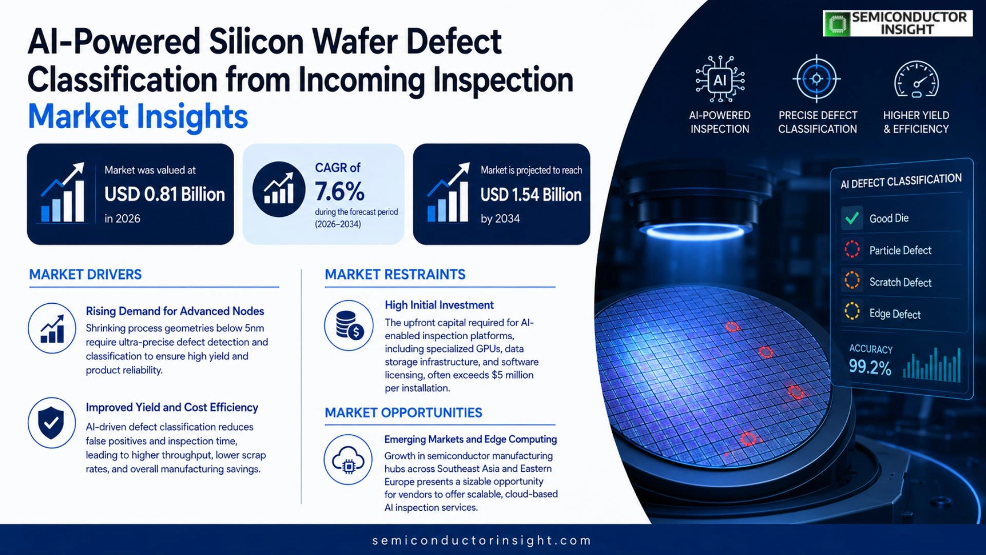
MARKET DRIVERS
Technological Advancements Driving Adoption
The rapid maturation of machine‑learning algorithms and high‑resolution imaging sensors has created a fertile environment for AI-Powered Silicon Wafer Defect Classification from Incoming Inspection Market. Deep‑learning models now achieve sub‑micron defect detection accuracy, enabling fabs to identify pattern variations that were previously invisible to conventional rule‑based systems.
Cost Efficiency and Yield Improvement
By automating defect classification, manufacturers reduce reliance on manual expertise, cutting labor costs by an estimated 20‑25 %. Moreover, early detection of critical defects improves overall wafer yield, translating into annual savings that often exceed $10 million for mid‑size fabs.
➤ AI-driven inspection can lower false‑positive rates by roughly 30 % while boosting true‑positive identification, directly enhancing production efficiency.
These drivers collectively accelerate investment cycles, prompting leading semiconductor equipment vendors to embed AI modules into next‑generation inspection tools, thereby expanding the addressable market base.
MARKET CHALLENGES
Integration Complexity
Implementing AI solutions within existing fab lines often requires retrofitting legacy hardware and harmonizing data formats from disparate metrology tools. The resulting integration timeline can extend beyond 12 months, discouraging smaller players with tighter capital constraints.
Other Challenges
Data Scarcity
High‑quality, labeled defect datasets remain limited, especially for emerging node technologies. Without sufficient training data, model generalization suffers, leading to inconsistent classification performance across product families.
MARKET RESTRAINTS
High Initial Investment
The upfront capital required for AI‑enabled inspection platforms,including specialized GPUs, data storage infrastructure, and software licensing,often exceeds $5 million per installation. This financial barrier limits rapid adoption, particularly among fab operators focusing on short‑term ROI.
MARKET OPPORTUNITIES
Emerging Markets and Edge Computing
Growth in semiconductor manufacturing hubs across Southeast Asia and Eastern Europe presents a sizable opportunity for vendors to offer scalable, cloud‑based AI inspection services. Edge‑deployed inference engines further reduce latency, enabling real‑time defect classification directly on the production line.
AI-Powered Silicon Wafer Defect Classification from Incoming Inspection Market Trends
Accelerated Adoption Through Integrated AI Analytics
The shift toward AI-driven inspection is reshaping quality control in semiconductor fabs. By embedding deep‑learning models into incoming wafer inspection stations, manufacturers can classify particles, scratches and lattice anomalies in real time. This automation shortens the manual review cycle from hours to minutes, allowing production lines to maintain higher throughput without sacrificing accuracy. Recent deployments show yield predictability improving by double‑digit percentages, while defect‑related downtime drops noticeably. The trend is reinforced by a growing portfolio of AI accelerators that fit within existing equipment footprints, making the technology accessible to both leading and midsize fabs. In parallel, fabs expanding capacity for advanced nodes report that AI‑supported inspection reduces scrap rates by up to 12%, aligning with the push for higher volume production at lower cost per wafer. These efficiency gains are especially pronounced in automotive power‑electronics lines, where defect tolerance is minimal.
Other Trends
Strategic Alliances Accelerate Solution Maturity
Partnerships between equipment makers and AI specialists have become a catalyst for rapid market maturation. In March 2024, KLA Corporation announced a joint effort with NVIDIA to integrate GPU‑accelerated inference engines directly into its inspection platforms, delivering sub‑millisecond decision latency. Applied Materials introduced an end‑to‑end AI inspection suite that combines sensor fusion with cloud‑based analytics, enabling users to benchmark defect patterns across multiple fabs. These collaborations reduce development cycles and lower the barrier to entry for AI adoption, as fabs can leverage proven hardware while focusing on process‑specific model tuning. As a result, the ecosystem now supports a broader range of defect classes, from nanoscale particles to complex lattice distortions, strengthening overall yield assurance.
Future Outlook Emphasizes Integrated Quality Metrics
Looking ahead, the market is expected to consolidate around platforms that couple high‑resolution imaging with scalable AI inference. Fab managers are prioritizing solutions that provide actionable quality metrics directly within manufacturing execution systems, reducing the need for separate data pipelines. The convergence of tighter automotive and mobile reliability standards with the cost pressures of advanced‑node production creates a compelling business case for continuous AI monitoring. Companies that align their product roadmaps with these requirements,by offering modular upgrades, extensive model libraries, and transparent performance dashboards,are likely to capture the majority of upcoming spend. Consequently, the AI‑Powered Silicon Wafer Defect Classification from Incoming Inspection Market will remain a focal point of technology investment across the semiconductor value chain. Overall, the trajectory indicates sustained investment as AI becomes integral to wafer quality assurance.
COMPETITIVE LANDSCAPE
Key Industry Players
AI‑Powered Silicon Wafer Defect Classification – Competitive Overview
KLA Corp remains the de‑facto market leader in AI‑enhanced incoming wafer inspection, leveraging its extensive metrology portfolio and recent collaboration with NVIDIA to embed GPU‑accelerated inference engines directly into inspection tools. This partnership accelerates real‑time defect classification and has set a benchmark for integration depth that rivals such as Applied Materials are quickly matching. Applied Materials’ AI inspection suite, introduced in 2024, bundles proprietary deep‑learning models with its deposition and etch equipment, allowing seamless data flow across the fab floor. ASML, while historically focused on lithography, has entered the niche by offering pattern‑recognition add‑ons for its metrology modules, further consolidating the top‑tier ecosystem. The market structure reflects a tri‑pole of KLA, Applied Materials, and ASML, each commanding a sizable share of high‑volume fabs that demand end‑to‑end, AI‑driven yield analytics.
Beyond the leading trio, a vibrant cohort of specialized vendors enriches the competitive landscape. Tokyo Electron and Lam Research provide AI‑ready inspection sensors that complement their process equipment, targeting mid‑size fabs seeking modular upgrades. Companies such as Camtek, Onto Innovation, and Cohu focus on niche defect‑type classifiers, often integrating proprietary neural networks for particle and scratch detection. Meanwhile, Hitachi High‑Technologies, Advantest, and Teradyne supply AI‑powered test and measurement platforms that feed defect data into broader quality‑control systems. Smaller innovators like MKS Instruments and 3M’s semiconductor division contribute specialty optics and surface‑treatment technologies that enhance image fidelity, thereby improving classification accuracy across the value chain.
List of Key AI-Powered Silicon Wafer Defect Classification Companies Profiled
- KLA Corp
- Applied Materials
- ASML Holding
- NVIDIA
- Tokyo Electron
- Lam Research
- Camtek
- Onto Innovation
- Cohu
- Hitachi High‑Technologies
- Advantest
- Teradyne
- MKS Instruments
- 3M Semiconductor
Segment Analysis:
| Segment Category | Sub-Segments | Key Insights |
| By Type |
|
Convolutional Neural Network based classifiers dominate because they directly map high‑resolution wafer images to defect categories. • Offer rapid inference suitable for inline inspection. • Align well with existing image‑processing pipelines in fabs. • Provide a clear path for continuous improvement through additional labeled data. |
| By Application |
|
Particle defect detection is the leading application as manufacturers prioritize removal of contaminant‑induced yield loss. • AI models quickly isolate sub‑micron particles that traditional heuristics miss. • Enhances root‑cause analysis by linking particle morphology to process steps. • Supports tighter specification compliance for automotive and mobile semiconductor supplies. |
| By End User |
|
Foundries lead the adoption curve due to scale‑driven pressure for consistent yields across multiple customers. • AI‑driven classification fits within their multi‑tenant quality platforms. • Enables rapid onboarding of new node technologies with minimal re‑engineering. • Facilitates collaborative data sharing while preserving IP confidentiality. |
| By Technology |
|
GPU‑accelerated inference engines are favored because they balance high throughput with flexibility for model updates. • Provide the computational headroom required for real‑time defect scoring. • Allow integration of emerging deep‑learning architectures without hardware redesign. • Benefit from ecosystem support, illustrated by partnerships such as KLA with NVIDIA. |
| By Deployment |
|
On‑premise integrated inspection stations remain dominant as fabs require deterministic latency and data sovereignty. • Direct connectivity to wafer handling equipment eliminates data transport delays. • Ensures compliance with strict security policies for proprietary process data. • Supports incremental upgrades without disrupting existing production lines. |
Regional Analysis: AI-Powered Silicon Wafer Defect Classification from Incoming Inspection Market
Silicon Valley and Boston host a concentration of AI start‑ups that specialize in defect‑pattern recognition, fostering rapid prototyping and integration with existing fab software stacks.
Near‑shore logistics and a robust semiconductor supply chain enable timely delivery of AI‑enhanced inspection equipment, reducing downtime for manufacturers.
Government initiatives such as the CHIPS Act provide financial incentives that lower the entry barrier for AI‑driven wafer inspection technologies.
A deep talent pool in machine learning, computer vision, and semiconductor physics ensures continuous innovation and skilled workforce availability.
Europe
European fabs are emphasizing sustainability and precision, prompting a measured uptake of AI‑Powered Silicon Wafer Defect Classification solutions. Germany and the Netherlands lead with pilot projects that integrate machine‑learning models into existing inspection lines, aiming to lower waste and improve yield. Industry consortia backed by the European Commission facilitate knowledge sharing and standardisation across borders, while regulatory bodies encourage data‑driven process optimisation. Although adoption is cautious, the focus on high‑end automotive and IoT chips drives steady interest in advanced defect‑classification tools.
Asia‑Pacific
The Asia‑Pacific region exhibits rapid expansion, propelled by large‑scale fabs in Taiwan, South Korea, and China. Manufacturers are increasingly turning to AI‑enabled inspection to manage the high volume of wafers while maintaining stringent quality standards. Collaborative research programmes between chipmakers and local AI firms accelerate algorithm refinement for region‑specific defect patterns. Cost‑effectiveness remains a key driver, as operators seek to balance capital expenditure with the productivity gains offered by automated classification.
South America
South American semiconductor activity is emerging, with Brazil and Chile investing in niche production lines for specialty devices. The market for AI‑Powered Silicon Wafer Defect Classification is still nascent, yet early adopters appreciate the technology’s ability to compensate for limited manual expertise. Partnerships with North American technology providers are common, facilitating technology transfer and training. As regional demand for advanced electronics grows, investment in AI‑driven inspection is expected to gain momentum.
Middle East & Africa
In the Middle East and Africa, strategic initiatives aim to diversify economies through advanced manufacturing. Pilot installations in the United Arab Emirates and South Africa are exploring AI‑based wafer inspection to support growing semiconductor assembly capabilities. Emphasis is placed on building local expertise and leveraging cloud‑based AI services to offset infrastructure constraints. While market penetration remains modest, the focus on high‑value, low‑volume production creates a niche for sophisticated defect‑classification solutions.
Report Scope
This market research report provides a comprehensive analysis of the AI-Powered Silicon Wafer Defect Classification from Incoming Inspection Market , covering the forecast period 2026–2034. It offers detailed insights into market dynamics, technological advancements, competitive landscape, and key trends shaping the industry.
Key focus areas of the report include:
- Market Overview: The report begins with an overview outlining its current market scenario, key growth indicators, and industry transformation drivers. It discusses macroeconomic factors, demand–supply balance, regulatory landscape, and the strategic role of semiconductors in powering advancements across industries such as automotive, telecommunications, consumer electronics, and industrial automation.
- Market Size & Forecast: Historical data and future projections for revenue, unit shipments, and market value across major regions and segments.
- Segmentation Analysis: Detailed breakdown by product type, technology, application, and end-user industry to identify high-growth segments and investment opportunities.
- Regional Insights: Insights into market performance across North America, Europe, Asia-Pacific, Latin America, and the Middle East & Africa, including country-level analysis where relevant.
- Competitive Landscape: Profiles of leading market participants, including their product offerings, R&D focus, manufacturing capacity, pricing strategies, and recent developments such as mergers, acquisitions, and partnerships.
- Technology Trends & Innovation: Assessment of emerging technologies, integration of AI/IoT, semiconductor design trends, fabrication techniques, and evolving industry standards.
- Market Drivers & Restraints: Evaluation of factors driving market growth along with challenges, supply chain constraints, regulatory issues, and market-entry barriers.
- Stakeholder Insights: Insights for component suppliers, OEMs, system integrators, investors, and policymakers regarding the evolving ecosystem and strategic opportunities.
Primary and secondary research methods are employed, including interviews with industry experts, data from verified sources, and real-time market intelligence to ensure the accuracy and reliability of the insights presented.
FREQUENTLY ASKED QUESTIONS:
What is the current market size of AI-Powered Silicon Wafer Defect Classification from Incoming Inspection Market?
-> AI-Powered Silicon Wafer Defect Classification from Incoming Inspection market size is projected to grow from USD 0.81 billion in 2026 to USD 1.54 billion by 2034.
Which key companies operate in AI-Powered Silicon Wafer Defect Classification from Incoming Inspection Market?
-> Key players include KLA Corp, NVIDIA, Applied Materials, among others.
What are the key growth drivers?
-> Key growth drivers include expansion of advanced‑node fabs, rising demand for higher yields, adoption of AI analytics in wafer inspection, and stringent quality standards in automotive and mobile sectors.
Which region dominates the market?
-> Asia-Pacific is the fastest‑growing region, while North America holds a significant share due to major semiconductor hubs.
What are the emerging trends?
-> Emerging trends include GPU‑accelerated inference engines, integrated AI inspection suites, and real‑time defect analytics platforms.

Get Sample Report PDF for Exclusive Insights
Report Sample Includes
- Table of Contents
- List of Tables & Figures
- Charts, Research Methodology, and more...
 Download Sample Report PDF




