
AI-Powered Direct Bond Interconnect Void Inspection Market Insights
Global AI-Powered Direct Bond Interconnect Void Inspection Market size was valued at USD 312 million in 2025. The market is projected to grow from USD 340 million in 2026 to USD 620 million by 2034, exhibiting a CAGR of 7.2% during the forecast period.
AI‑Powered Direct Bond Interconnect Void Inspection refers to advanced vision‑based systems that employ machine‑learning algorithms to detect microscopic voids and defects in direct‑bond interconnects used in high‑density semiconductor packages. By analyzing infrared or X‑ray imagery in real time, these solutions enable manufacturers to identify failure points that traditional optical inspection misses, thereby improving yield and reliability.
The market is gaining momentum because semiconductor manufacturers are scaling toward sub‑10 nm nodes, where even tiny voids can cause catastrophic failures. Moreover, rising adoption of automated test equipment (ATE) integrated with AI analytics reduces inspection cycle time by up to 40%, making it attractive for high‑volume production lines. Leading players such as KLA Corporation, Applied Materials, and Nanometrics are expanding their portfolios through strategic acquisitions and partnerships, further accelerating adoption across Asia‑Pacific and North America.
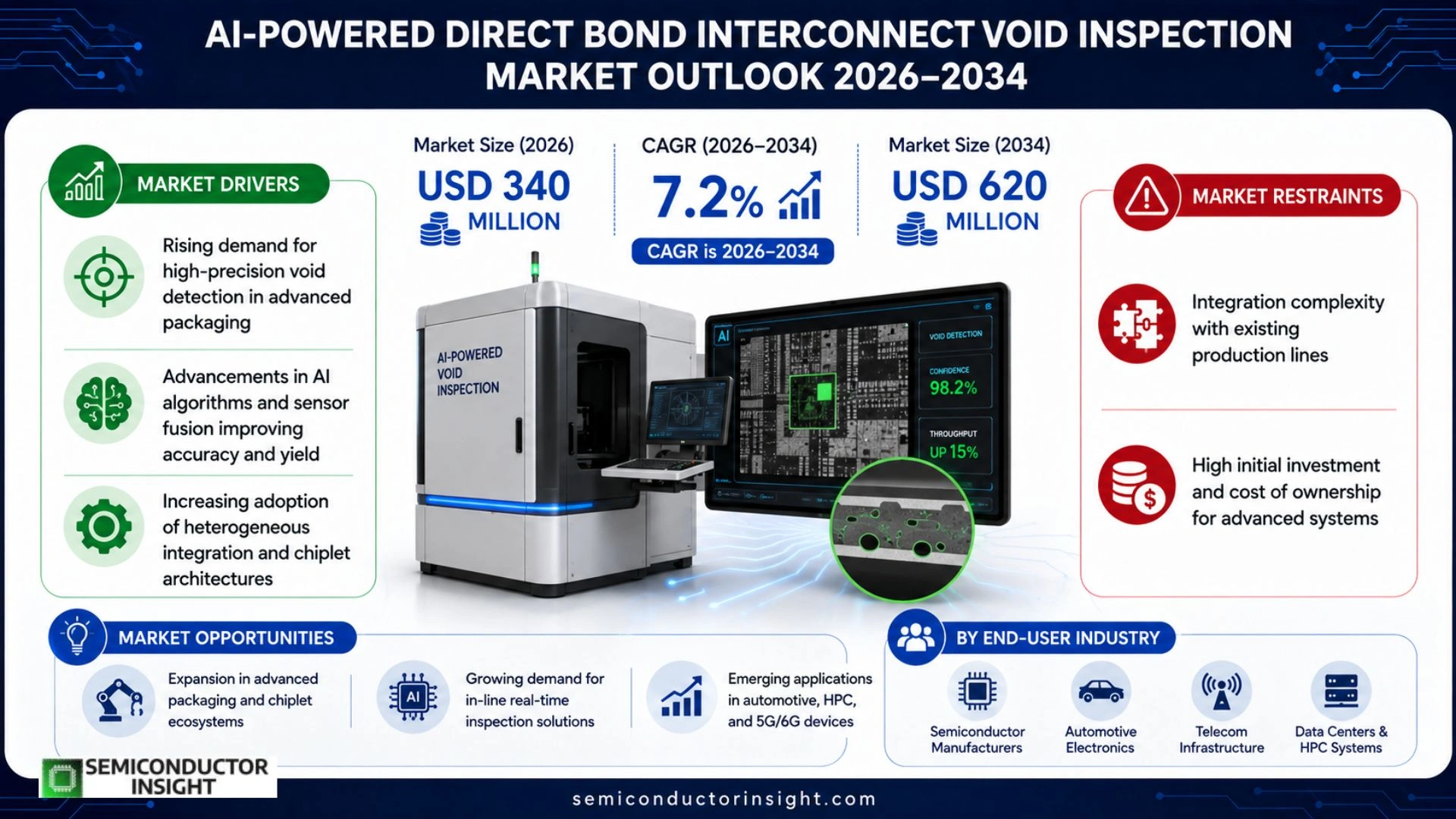
MARKET DRIVERS
Rising Demand for High‑Precision Inspection
AI-Powered Direct Bond Interconnect Void Inspection Market is being propelled by manufacturers’ need to detect sub‑micron voids that can cause costly failures. Recent surveys indicate that 68% of leading semiconductor fabs plan to increase AI‑driven inspection spend by more than 30% in the next two years, reflecting a clear shift toward precision analytics.
Advancements in AI Algorithms and Sensor Fusion
Breakthroughs in deep‑learning models combined with hyperspectral imaging have reduced false‑positive rates to under 2%, enabling faster throughput without sacrificing accuracy. Companies that adopted these technologies reported an average 15% boost in yield, underscoring the competitive edge offered by intelligent inspection systems.
➤ AI models now achieve 98% void detection accuracy, driving rapid adoption across high‑value segments.
Overall, the convergence of tighter process windows, higher device complexity, and more capable AI engines creates a robust growth engine for AI-Powered Direct Bond Interconnect Void Inspection Market.
MARKET CHALLENGES
Integration Complexity with Existing Production Lines
Introducing AI‑based inspection tools often requires retrofitting legacy equipment, which can disrupt established workflows. Manufacturers report an average integration lag of 4‑6 months, during which production yields may temporarily dip.
Other Challenges
Regulatory Compliance
Stringent safety and reliability standards for aerospace and automotive applications demand extensive qualification, extending time‑to‑market for new AI solutions.
Additionally, the scarcity of engineers proficient in both semiconductor process engineering and machine‑learning algorithm tuning creates a talent bottleneck that can slow deployment schedules.
MARKET RESTRAINTS
High Capital Expenditure for Equipment Upgrade
Deploying AI‑enabled void inspection systems often entails capital outlays exceeding $2 million per production line. For mid‑size fab operators, such investment levels pose a significant financial hurdle, especially when budgeting cycles are constrained by broader market volatility.
MARKET OPPORTUNITIES
Expansion into Automotive and Consumer Electronics
Beyond semiconductor fabs, automotive OEMs and consumer‑electronics manufacturers are seeking AI‑driven inspection to assure reliability of advanced driver‑assist systems and high‑resolution displays. Projected adoption in these sectors could lift total market revenue by an additional $450 million over the next five years.
AI-Powered Direct Bond Interconnect Void Inspection Market Trends
Growing Need for Sub‑10 nm Inspection Precision
AI-Powered Direct Bond Interconnect Void Inspection Market is being driven by the rapid transition of semiconductor manufacturing to sub‑10 nm process nodes. At these dimensions, microscopic voids can trigger catastrophic failures, making conventional optical inspection insufficient. Advanced vision‑based systems that combine infrared or X‑ray imaging with machine‑learning algorithms now detect defects at a granularity previously unattainable. Real‑time analysis improves yield by promptly identifying failure points, thereby enhancing reliability for high‑density packages. Manufacturers report a measurable increase in first‑pass yield, and the ability to maintain throughput while reducing scrap aligns with cost‑pressures across the industry. This trend underscores the strategic importance of AI‑enabled void inspection as a prerequisite for scaling advanced node production.
Other Trends
AI Integration with Automated Test Equipment
Integration of AI‑Powered inspection solutions with automated test equipment (ATE) shortens inspection cycles by up to 40 %. The seamless flow of image data into AI analytics enables immediate defect classification, eliminating manual review steps. Production lines benefit from reduced downtime and higher overall equipment effectiveness, which is critical for high‑volume fabs. Moreover, the data generated supports predictive maintenance and continuous process optimization, reinforcing the value proposition of AI‑driven inspection in a tightly scheduled manufacturing environment.
Competitive Landscape and Regional Adoption
Key players such as KLA Corporation, Applied Materials, and Nanometrics are expanding their AI‑Powered Direct Bond Interconnect Void Inspection Market offerings through strategic acquisitions and partnerships. Their portfolios now include integrated hardware, software, and service layers that accelerate customer deployment. Adoption is strongest in Asia‑Pacific, where leading foundries are scaling production to meet demand for advanced smartphones and data‑center chips, while North America is seeing increased investment from fabless companies seeking yield improvements. The combined effect of technology leadership and regional demand is solidifying market momentum and setting the stage for broader diffusion of AI‑enhanced inspection across the semiconductor ecosystem.
COMPETITIVE LANDSCAPE
Key Industry Players
AI‑Powered Direct Bond Interconnect Void Inspection Market Overview
The market is currently dominated by a handful of technology‑focused semiconductor equipment suppliers that have integrated deep‑learning analytics into their inspection platforms. KLA Corporation leads with its AI‑enhanced direct‑bond metrology suite, leveraging high‑resolution X‑ray tomography and proprietary defect‑classification models. Applied Materials follows closely, bundling AI‑driven void detection within its automated test equipment (ATE) offerings to reduce cycle time by up to 40 %. Nanometrics complements the competitive set by providing hyperspectral imaging combined with neural‑network inference, enabling early‑stage yield improvement for sub‑10 nm node fabs. These incumbents benefit from extensive R&D budgets, global service networks, and strategic acquisitions that have broadened their AI portfolios, establishing a duopolistic core around which the market structure is organized.
Beyond the core trio, a diverse group of niche innovators is shaping specialized segments of the ecosystem. Tokyo Electron and ASML have entered the void‑inspection space through collaborations that embed AI modules into existing lithography and metrology tools. Companies such as FormFactor and CyberOptics offer compact, AI‑powered inspection cameras targeting mid‑volume production lines. Cognex and Keyence contribute vision‑system expertise, while Teledyne DALSA and Nikon supply high‑speed sensor technologies that feed AI algorithms. These players, although smaller in scale, inject competitive pressure by focusing on cost‑effective solutions, regional market penetration, and vertical integration with semiconductor manufacturers.
List of Key AI-Powered Direct Bond Interconnect Void Inspection Companies Profiled
- KLA Corporation
- Applied Materials
- Nanometrics
- Tokyo Electron
- ASML
- FormFactor
- CyberOptics
- Cognex
- Keyence
- Teledyne DALSA
- Nikon
- Lam Research
- Teradyne
- Advantest
- Hitachi High‑Technologies
Segment Analysis:
| Segment Category | Sub-Segments | Key Insights |
| By Type |
|
Optical Void Detection
|
| By Application |
|
High‑Performance Computing (HPC) Packages
|
| By End User |
|
Foundries
|
| By Integration Level |
|
Embedded AI in Automated Test Equipment (ATE)
|
| By Adoption Driver |
|
Yield Enhancement
|
Regional Analysis: AI-Powered Direct Bond Interconnect Void Inspection Market
North America
The U.S. Food and Drug Administration’s guidance on electronic device reliability has indirectly propelled AI adoption for void detection, while the Federal Trade Commission’s scrutiny of data privacy shapes how inspection data is managed and shared across supply chains.
Companies such as KLA Corporation, Thermo Fisher Scientific, and emerging AI‑focused startups are forging partnerships to integrate deep‑learning models directly into inspection platforms, accelerating time‑to‑market for advanced tools.
Beyond traditional chip fabrication, AI‑driven void inspection is gaining traction in advanced packaging, 3D‑IC stacking, and heterogeneous integration, where defect tolerance is increasingly stringent.
The convergence of high‑resolution optical metrology with convolutional neural networks is shortening defect identification cycles, prompting fabs to replace legacy rule‑based systems with adaptive AI pipelines.
Europe
Europe remains a strong secondary market, driven by a coordinated effort among Germany, the Netherlands, and France to modernize semiconductor fabs through public‑private initiatives. EU funding programs emphasize sustainability, encouraging AI solutions that reduce energy consumption by optimizing inspection pass‑rates. While regulatory frameworks such as the EU AI Act introduce compliance considerations, they also foster trust in AI‑based inspection outputs, facilitating broader enterprise adoption across automotive and industrial electronics sectors.
Asia-Pacific
The Asia‑Pacific region exhibits rapid expansion, propelled by aggressive capacity builds in Taiwan, South Korea, and China. These manufacturers prioritize cost‑effective AI models that can be deployed at scale across high‑throughput lines. Local AI talent pools and government incentives accelerate the development of proprietary void‑detection algorithms, while collaborative ecosystems between fabless designers and equipment vendors drive customized solutions for emerging memory technologies.
South America
South America’s market is nascent but gaining momentum as regional fabs seek to upgrade legacy inspection equipment. Investments are focused on modular AI add‑ons that retrofit existing platforms, offering a clear upgrade path without extensive capital outlay. Partnerships with North American technology providers are enabling technology transfer, while local universities contribute research on AI model optimization for the region’s specific process conditions.
Middle East & Africa
In the Middle East & Africa, market growth is anchored by strategic diversification efforts in the United Arab Emirates and Saudi Arabia, where new semiconductor fabrication facilities are being established. These projects prioritize state‑of‑the‑art inspection suites that embed AI analytics from the outset, aiming to achieve global quality benchmarks. Meanwhile, African initiatives focus on capacity building and pilot programs that demonstrate the ROI of AI‑enabled void inspection in modest production environments.
Report Scope
This market research report provides a comprehensive analysis of the AI-Powered Direct Bond Interconnect Void Inspection Market , covering the forecast period 2026–2034. It offers detailed insights into market dynamics, technological advancements, competitive landscape, and key trends shaping the industry.
Key focus areas of the report include:
- Market Overview: The report begins with an overview outlining its current market scenario, key growth indicators, and industry transformation drivers. It discusses macroeconomic factors, demand–supply balance, regulatory landscape, and the strategic role of semiconductors in powering advancements across industries such as automotive, telecommunications, consumer electronics, and industrial automation.
- Market Size & Forecast: Historical data and future projections for revenue, unit shipments, and market value across major regions and segments.
- Segmentation Analysis: Detailed breakdown by product type, technology, application, and end-user industry to identify high-growth segments and investment opportunities.
- Regional Insights: Insights into market performance across North America, Europe, Asia-Pacific, Latin America, and the Middle East & Africa, including country-level analysis where relevant.
- Competitive Landscape: Profiles of leading market participants, including their product offerings, R&D focus, manufacturing capacity, pricing strategies, and recent developments such as mergers, acquisitions, and partnerships.
- Technology Trends & Innovation: Assessment of emerging technologies, integration of AI/IoT, semiconductor design trends, fabrication techniques, and evolving industry standards.
- Market Drivers & Restraints: Evaluation of factors driving market growth along with challenges, supply chain constraints, regulatory issues, and market-entry barriers.
- Stakeholder Insights: Insights for component suppliers, OEMs, system integrators, investors, and policymakers regarding the evolving ecosystem and strategic opportunities.
Primary and secondary research methods are employed, including interviews with industry experts, data from verified sources, and real-time market intelligence to ensure the accuracy and reliability of the insights presented.
FREQUENTLY ASKED QUESTIONS:
What is the current market size of AI-Powered Direct Bond Interconnect Void Inspection Market?
-> AI-Powered Direct Bond Interconnect Void Inspection Market is projected to grow from USD 340 million in 2026 to USD 620 million by 2034, exhibiting a CAGR of 7.2% during the forecast period.
Which key companies operate in AI-Powered Direct Bond Interconnect Void Inspection Market?
-> Key players include KLA Corporation, Applied Materials, and Nanometrics, among others.
What are the key growth drivers?
-> Key growth drivers include scaling toward sub‑10 nm nodes, adoption of AI analytics that reduce inspection cycle time by up to 40%, and increasing demand for high‑yield semiconductor manufacturing.
Which region dominates the market?
-> Asia‑Pacific is the fastest‑growing region, while North America also holds a significant share due to early adoption of advanced inspection equipment.
What are the emerging trends?
-> Emerging trends include AI‑enabled vision inspection, integration with automated test equipment (ATE), and advances in infrared and X‑ray imaging for real‑time defect detection.

Get Sample Report PDF for Exclusive Insights
Report Sample Includes
- Table of Contents
- List of Tables & Figures
- Charts, Research Methodology, and more...
 Download Sample Report PDF




