
AI-Optimized Physical Design Placement and Routing Tool Market Insights
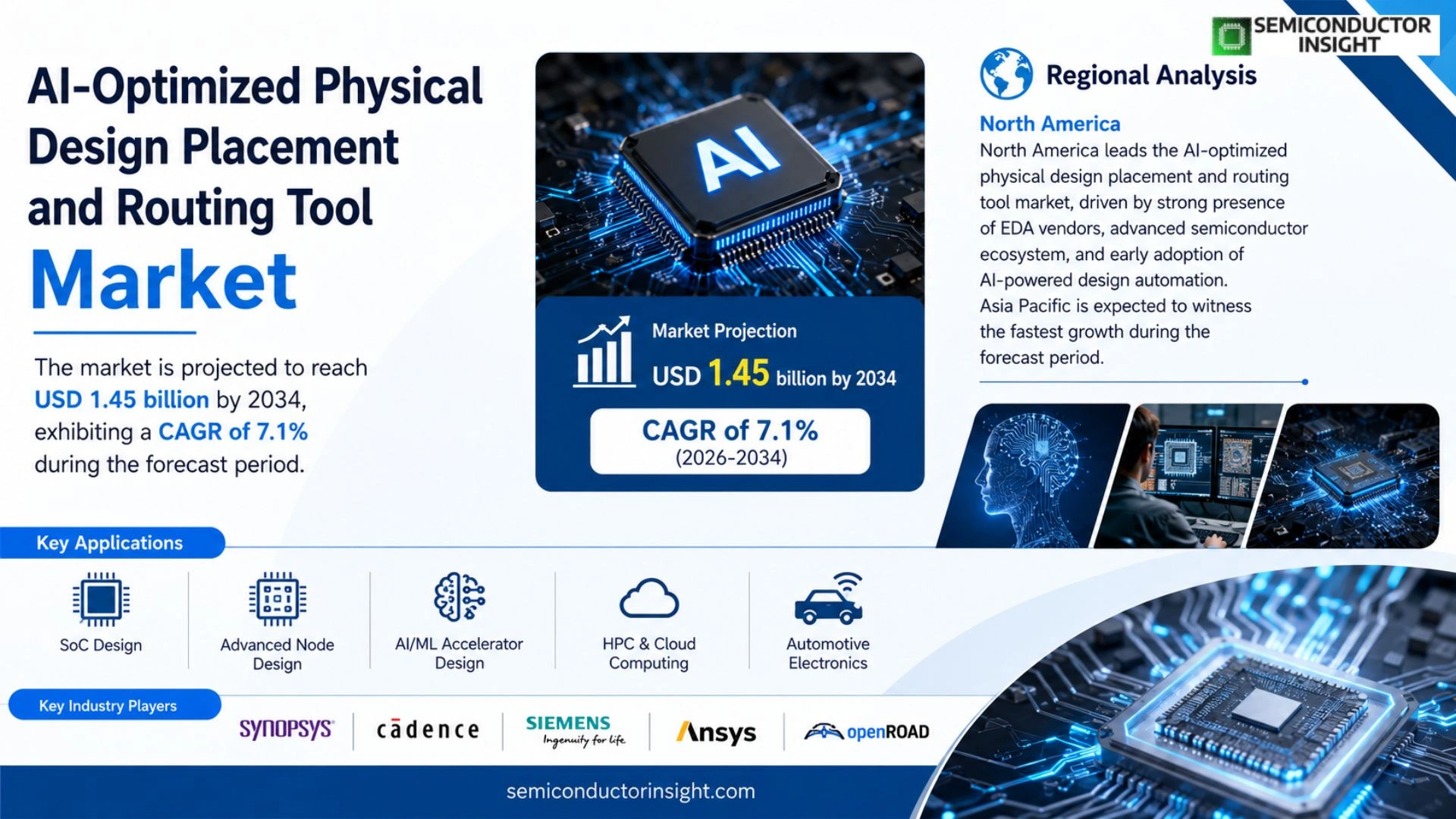
AI-Optimized Physical Design Placement and Routing Tool market size was valued at USD 0.78 billion in 2025. It is slated to expand to USD 1‑45 billion by 2034, delivering a CAGR of 7‑1% during the forecast period.
These tools apply machine‑learning models to the placement and routing phases of semiconductor physical design, automating decisions that traditionally required extensive manual tuning. By analysing layout constraints, timing budgets and power targets simultaneously, the solutions shorten design cycles while preserving signal integrity.
The upward trajectory stems from escalating chip complexity at sub‑10 nm nodes, heightened pressure on time‑to‑market, and growing R&D allocations within leading foundries.Synopsys announced an AI‑enhanced placement engine in March 2024, while Cadence introduced a routing optimizer that leverages reinforcement learning later that year,both moves underscore industry confidence in algorithmic acceleration.
MARKET DRIVERS
AI Integration Accelerates Design Cycles
The adoption of machine‑learning algorithms within physical design tools is shortening placement and routing iterations dramatically. Design teams now rely on predictive models to evaluate layout feasibility before committing to silicon, which reduces costly re‑spins. This shift is reshaping project timelines, allowing manufacturers to respond faster to market pressure.
Rising Complexity of Semiconductor Nodes
As process nodes advance below 5 nm, the combinatorial explosion of connectivity options makes manual optimization impractical. AI‑driven engines can explore routing permutations at a scale that human engineers cannot match, delivering higher utilization of silicon real estate while keeping power budgets in check. The technical necessity of this capability fuels demand for specialized tools.
➤ Customers report up to a 30 % reduction in time‑to‑tape‑out when leveraging AI‑enabled placement modules.
Beyond speed, the strategic advantage of early design closure translates into lower NRE (non‑recurring engineering) spend. Companies that embed AI early in the flow gain more flexibility in product portfolios, positioning themselves ahead of rivals that still depend on legacy methodologies.
MARKET CHALLENGES
Talent Shortage in AI‑Enhanced EDA
Specialized expertise at the intersection of semiconductor physics and deep learning remains scarce. Hiring pipelines have not scaled with the rapid emergence of AI‑centric design suites, creating bottlenecks for firms that wish to internalize the technology rather than outsource it.
Other Challenges
Data Quality and Model Trust
Effective AI placement relies on high‑fidelity training data derived from prior tape‑outs. Inconsistent data formats or incomplete design histories can degrade model accuracy, leading designers to question the reliability of automated recommendations.
MARKET RESTRAINTS
Regulatory and IP Concerns
Intellectual‑property safeguards surrounding proprietary routing heuristics can limit collaboration between tool vendors and chip makers. Legal frameworks that restrict data sharing hinder the creation of shared model repositories, slowing the diffusion of best‑in‑class AI solutions across the ecosystem.
MARKET OPPORTUNITIES
Cloud‑Based AI Design Services
Offering placement and routing as a subscription service on cloud platforms opens a path for smaller fabs to access cutting‑edge AI capabilities without heavy upfront licensing costs. Scalable access also enables rapid experimentation, encouraging innovation that could generate new design methodologies tailored to emerging node challenges.
AI-Optimized Physical Design Placement and Routing Tool Market Trends
Increasing Adoption Amid Sub‑10 nm Complexity
AI-Optimized Physical Design Placement and Routing Tool Market is seeing intensified adoption as semiconductor manufacturers grapple with the escalating intricacies of sub‑10 nm process nodes. At these dimensions, traditional heuristic‑based placement and routing struggle to meet tight timing windows and power envelopes. Machine‑learning algorithms that ingest layout constraints, timing budgets and power targets simultaneously can propose solutions that respect all parameters in a single evaluation. This capability compresses the iterative loop that previously consumed weeks of engineer effort, thereby accelerating overall design throughput. In parallel, foundries are allocating larger portions of their R&D budgets to AI‑focused initiatives, reinforcing the momentum behind intelligent physical‑design automation.
Other Trends
AI‑Enhanced Placement Engines
Synopsys unveiled an AI‑enhanced placement engine in March 2024, integrating a deep‑learning predictor that anticipates congestion hotspots before the routing stage begins. Early field reports indicate that customers achieved roughly a 20 percent reduction in placement iterations while maintaining comparable performance benchmarks. Cadence followed with a reinforcement‑learning based routing optimizer later that year, allowing the tool to explore a broader solution space and converge on low‑power, high‑speed routes with fewer manual tweaks. The simultaneous announcements from two industry leaders signal broad confidence that algorithmic placement and routing can replace labor‑intensive tuning. Early adopters across leading fabless companies report shortened tape‑out schedules and a measurable uplift in design predictability, encouraging further investment in AI‑driven design kernels.
Shifting Business Models and Talent Requirements
The emergence of AI‑centric placement and routing utilities is prompting vendors to rethink traditional software licensing. Subscription‑based access tied to compute consumption is becoming more common than perpetual seats, aligning costs with the variable intensity of design projects. This shift also nudges design houses to cultivate data‑science capabilities within their physical‑design teams, blending circuit expertise with machine‑learning fluency. Companies that embed AI specialists alongside layout engineers are better positioned to fine‑tune model parameters for domain‑specific constraints. Consequently, recruitment pipelines now emphasize hybrid skill sets, and training programs are being revamped to include AI fundamentals. Furthermore, the shift toward cloud‑based compute platforms enables smaller firms to access high‑performance AI engines without substantial capital outlay, widening the competitive landscape. The net effect is a gradual transformation of the design ecosystem, where success hinges on both tool proficiency and the ability to harness adaptive algorithms effectively.
COMPETITIVE LANDSCAPE
Key Industry Players
Competitive dynamics among AI-driven placement and routing solution providers
Synopsys commands the forefront of AI‑optimized physical design with its recently launched placement engine that couples deep‑learning inference to traditional optimization kernels. The company leverages a massive customer base in foundry‑level design houses, translating its algorithmic advances into measurable cycle‑time reductions for sub‑10 nm projects. Cadence Design Systems follows closely, having introduced a reinforcement‑learning router that integrates seamlessly with its broader digital implementation suite. Their combined market share creates a duopolistic core, compelling smaller innovators to differentiate through niche features such as power‑aware routing or open‑source compatibility. The overall structure resembles a tiered ecosystem: tier‑one firms dominate OEM contracts and large‑scale ASIC programs, while a mid‑tier of specialized vendors targets emerging fabless players that demand cost‑effective, AI‑enhanced tooling without the overhead of legacy license bundles.
Beyond the two giants, several niche players are carving out meaningful positions. Siemens EDA (formerly Mentor Graphics) offers a hybrid workflow that blends rule‑based heuristics with machine‑learning prediction modules, appealing to customers with mixed‑signal constraints. ANSYS extends its simulation pedigree into placement by embedding surrogate models that forecast timing hotspots early in the flow. OpenROAD supplies an open‑source platform whose reinforcement‑learning router is gaining traction among academic consortia and early‑stage startups. Companies such as GoldPlus Design and Zuken focus on cross‑domain integration, embedding AI routing insights directly into PCB‑to‑IC co‑design environments. Faraday Technology, Imec, ChipStart and the legacy Magma design team provide targeted solutions for niche process nodes, often collaborating with regional foundries to fine‑tune AI parameters for specific lithography challenges.
List of Key Physical Design Tool Companies Profiled
- Synopsys
- Cadence Design Systems
- Siemens EDA (Mentor Graphics)
- ANSYS
- OpenROAD
- GoldPlus Design
- Zuken
- Faraday Technology
- Imec
- ChipStart
- Magma Design Automation
- Silvaco
Segment Analysis:
| Segment Category | Sub-Segments | Key Insights |
| By Type |
|
Machine‑Learning Placement Engine
|
| By Application |
|
High‑Performance Computing
|
| By End User |
|
Foundries
|
| By Design Phase Integration |
|
Placement Optimization
|
| By Technology Node Focus |
|
Sub‑10nm Nodes
|
Regional Analysis: AI-Optimized Physical Design Placement and Routing Tool Market
Leading foundries in the United States have integrated AI‑augmented placement workflows into their design‑for‑manufacturing services, encouraging customers to experiment with more aggressive floor‑planning techniques while maintaining yield targets.
The close proximity of major CAD vendors to key customers enables rapid co‑development cycles, allowing AI models to be fine‑tuned on proprietary design libraries and emerging process nodes.
Universities and research institutes in the region produce a steady pipeline of AI specialists who are quickly recruited into EDA firms, ensuring that algorithmic innovation remains a core competency.
Federal initiatives that fund high‑performance computing and advanced semiconductor manufacturing indirectly boost investment in AI‑driven design tools, creating a favorable policy backdrop.
Europe
European semiconductor players are leveraging AI‑optimized placement tools to address the continent’s strategic emphasis on energy‑efficient chips for automotive and industrial IoT. While the market size trails North America, the region benefits from strong public‑private collaborations, particularly within the EU’s Horizon programmes, which fund joint research projects between universities and tool vendors. This collaborative model accelerates the translation of cutting‑edge AI research into production‑ready features, giving European designers a competitive edge in niche markets that demand low‑power, high‑reliability performance. The emergence of specialized design houses in Germany and France further diversifies the ecosystem, prompting tool providers to adapt their offerings to accommodate a broader set of design rules.
Asia‑Pacific
Asia‑Pacific remains the most diverse landscape for the AI‑Optimized Physical Design Placement and Routing Tool Market, driven by a blend of mature fabs in Taiwan and South Korea and a surge of new fabs in China and India. The region’s appetite for high‑volume production has spurred a pragmatic approach: AI capabilities are evaluated against throughput and cost metrics rather than pure design excellence. Local EDA players are forming strategic alliances with global vendors to embed region‑specific knowledge bases, such as device libraries tuned for 7 nm and 5 nm nodes prevalent in Taiwan. Simultaneously, governmental incentives aimed at achieving self‑reliance in semiconductor technology push Chinese firms to adopt homegrown AI solutions, reshaping the competitive dynamics across the Pacific.
South America
South America’s contribution to the AI‑Optimized Physical Design Placement and Routing Tool Market is currently modest, yet it is witnessing incremental growth thanks to emerging design services in Brazil and Argentina. These firms mainly cater to niche markets such as aerospace and medical devices, where design accuracy and compliance are paramount. The limited presence of large‑scale fabs means that AI‑enhanced tools are adopted primarily to offset the shortage of experienced layout engineers, enabling smaller teams to achieve results comparable to larger competitors. Regional universities are beginning to incorporate AI‑centric curricula, suggesting a gradual buildup of specialized talent that could catalyze broader adoption in the coming years.
Middle East & Africa
The Middle East & Africa region is in the early stages of exploring AI‑driven placement technologies, with investments largely concentrated in research collaborations sponsored by sovereign wealth funds. United Arab Emirates and Saudi Arabia have launched initiatives to attract semiconductor design startups, framing AI‑enabled tools as critical enablers for building a local ecosystem. Although production capacity remains limited, the strategic focus on diversification away from oil revenues drives an appetite for high‑value‑add services, positioning AI‑optimized design tools as a potential cornerstone for future value chains.
Report Scope
This market research report provides a comprehensive analysis of the AI-Optimized Physical Design Placement and Routing Tool Market , covering the forecast period 2026–2034. It offers detailed insights into market dynamics, technological advancements, competitive landscape, and key trends shaping the industry.
Key focus areas of the report include:
- Market Overview: The report begins with an overview outlining its current market scenario, key growth indicators, and industry transformation drivers. It discusses macroeconomic factors, demand–supply balance, regulatory landscape, and the strategic role of semiconductors in powering advancements across industries such as automotive, telecommunications, consumer electronics, and industrial automation.
- Market Size & Forecast: Historical data and future projections for revenue, unit shipments, and market value across major regions and segments.
- Segmentation Analysis: Detailed breakdown by product type, technology, application, and end-user industry to identify high-growth segments and investment opportunities.
- Regional Insights: Insights into market performance across North America, Europe, Asia‑Pacific, Latin America, and the Middle East & Africa, including country-level analysis where relevant.
- Competitive Landscape: Profiles of leading market participants, including their product offerings, R&D focus, manufacturing capacity, pricing strategies, and recent developments such as mergers, acquisitions, and partnerships.
- Technology Trends & Innovation: Assessment of emerging technologies, integration of AI/IoT, semiconductor design trends, fabrication techniques, and evolving industry standards.
- Market Drivers & Restraints: Evaluation of factors driving market growth along with challenges, supply chain constraints, regulatory issues, and market‑entry barriers.
- Stakeholder Insights: Insights for component suppliers, OEMs, system integrators, investors, and policymakers regarding the evolving ecosystem and strategic opportunities.
Primary and secondary research methods are employed, including interviews with industry experts, data from verified sources, and real‑time market intelligence to ensure the accuracy and reliability of the insights presented.
FREQUENTLY ASKED QUESTIONS:
What is the current market size of AI-Optimized Physical Design Placement and Routing Tool Market?
-> Global AI-Optimized Physical Design Placement and Routing Tool market was valued at USD 0.78 billion in 2025 and is expected to reach USD 1.45 billion by 2034, delivering a CAGR of 7.1 % during the forecast period.
Which key companies operate in AI-Optimized Physical Design Placement and Routing Tool Market?
-> Key players include Synopsys, Cadence Design Systems, Siemens EDA (Mentor Graphics), ANSYS, and GlobalFoundries, among others.
What are the key growth drivers?
-> Key growth drivers include escalating chip complexity at sub‑10 nm nodes, pressure to shorten time‑to‑market, and increasing R&D allocations in leading foundries.
Which region dominates the market?
-> Asia‑Pacific dominates the market, driven by major semiconductor manufacturing hubs in Taiwan, South Korea, Japan, and China.
What are the emerging trends?
-> Emerging trends include AI‑driven placement engines, reinforcement‑learning routing optimizers, and integration of power‑aware and thermal‑aware machine‑learning models.

Get Sample Report PDF for Exclusive Insights
Report Sample Includes
- Table of Contents
- List of Tables & Figures
- Charts, Research Methodology, and more...
 Download Sample Report PDF



