
AI-Optimized Collective Die-to-Wafer Bonding Process Market Insights
AI-Optimized Collective Die-to-Wafer Bonding Process market size was valued at USD 210 million in 2025. The market is projected to grow from USD 225 million in 2026 to USD 520 million by 2034, exhibiting a CAGR of 9.1% during the forecast period.
AI‑Optimized Collective Die‑to‑Wafer bonding process integrates machine‑learning algorithms with conventional wafer‑level bonding equipment to dynamically adjust temperature, pressure, and alignment parameters in real time. By continuously analyzing sensor data, the system minimizes void formation and enhances bond strength across heterogeneous semiconductor stacks, enabling higher yields for advanced packaging such as heterogeneous integration and chiplet architectures.
The market is accelerating because semiconductor manufacturers are seeking higher throughput while reducing defect rates, especially as demand for high‑performance computing and automotive electronics surges. Moreover, recent collaborations,such as the partnership announced in March 2024 between a leading AI‑software provider and a major equipment OEM,to embed predictive analytics into bonding tools are driving adoption.
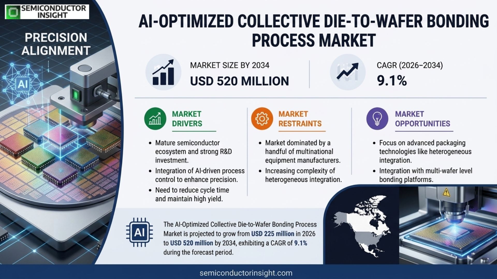
MARKET DRIVERS
Increasing Adoption of AI in Semiconductor Manufacturing
AI-Optimized Collective Die-to-Wafer Bonding Process Market is gaining momentum as chipmakers leverage machine‑learning algorithms to fine‑tune bonding parameters. Real‑time defect detection and predictive maintenance reduce cycle time, delivering higher yields that directly improve profitability.
Cost Efficiency Through Collective Bonding
By bonding multiple dies simultaneously, manufacturers lower material waste and equipment depreciation. The collective approach, when coupled with AI‑driven optimization, enables consistent pressure distribution, which translates into measurable cost savings across high‑volume production lines.
➤ “AI integration cuts average bonding defects by nearly 30 % while trimming cycle time by 15 %,”
These efficiency gains are prompting OEMs to prioritize platforms that support AI‑enhanced collective bonding, positioning the market for sustained growth over the next decade.
MARKET CHALLENGES
Technical Integration Barriers
Integrating advanced AI models with legacy bonding equipment requires bespoke software interfaces and skilled personnel. Many fabs face steep learning curves, which can delay deployment and inflate upfront costs.
Other Challenges
Supply Chain Constraints
The specialized sensors and high‑precision actuators needed for AI‑driven processes are sourced from a limited supplier base, creating potential bottlenecks that affect project timelines.
MARKET RESTRAINTS
Regulatory and Standards Uncertainty
Standardization bodies have yet to publish comprehensive guidelines for AI‑assisted die‑to‑wafer bonding, leading to divergent compliance requirements across regions. This uncertainty can discourage investment until clear regulatory pathways emerge.
Additionally, data‑privacy regulations governing the collection of process telemetry add layers of complexity for multinational operations, further restraining rapid market expansion.
Companies that proactively engage with standards committees are better positioned to mitigate these restraints and accelerate adoption.
MARKET OPPORTUNITIES
Emerging Applications in Advanced Packaging
The rise of heterogeneous integration and 3D‑IC architectures creates a fertile environment for AI‑optimized collective bonding. These applications demand sub‑micron alignment accuracy, a capability that AI algorithms can reliably deliver.
Furthermore, the growing focus on miniaturized medical and IoT devices expands the addressable market, as manufacturers seek cost‑effective bonding solutions that maintain high reliability at small form factors.
Strategic partnerships between AI software firms and equipment manufacturers are expected to unlock new product lines, driving long‑term value creation for AI-Optimized Collective Die-to-Wafer Bonding Process Market.
AI-Optimized Collective Die-to-Wafer Bonding Process Market Trends
AI-Driven Process Optimization Gains Traction
AI-Optimized Collective Die-to-Wafer Bonding Process Market is experiencing rapid adoption as semiconductor manufacturers embed machine‑learning algorithms directly into wafer‑level bonding tools. By continuously interpreting temperature, pressure and alignment sensor streams, the AI layer fine‑tunes process windows in real time, which reduces void formation and lifts bond strength across heterogeneous stacks. This capability underpins higher yields for chiplet‑based heterogeneous integration and other advanced packaging formats that dominate high‑performance computing and automotive electronics roadmaps. The result is a noticeable shift toward higher throughput lines that can maintain defect rates well below industry averages while supporting increasingly complex stack architectures.
Other Trends
Predictive Analytics Integration
A notable development occurred in March 2024 when a leading AI‑software provider announced a partnership with a major equipment OEM to embed predictive‑analytics modules into next‑generation bonding stations. The collaboration enables the system to forecast process drift before it impacts production, prompting automatic parameter correction that preserves throughput. Early adopters report a measurable improvement in cycle‑time consistency and a reduction in re‑work instances. This trend illustrates how AI-Optimized Collective Die-to-Wafer Bonding Process Market is moving from reactive control to proactive, data‑driven optimization, encouraging broader industry confidence in AI‑enhanced equipment portfolios.
Supply Chain and Ecosystem Consolidation
Concurrently, key players such as Applied Materials, Tokyo Electron and ASML are expanding their AI‑enabled bonding portfolios, creating a more consolidated ecosystem of hardware, software and services. The convergence reduces integration overhead for fab customers, who can now procure a single, AI‑augmented solution rather than stitching together disparate tools. This consolidation also accelerates standardization of data interfaces, making it easier for third‑party developers to contribute algorithms that target niche bonding challenges. As a result, the market is poised to sustain its momentum, driven by collaborative innovation and an ecosystem that lowers barriers to AI adoption across the semiconductor value chain.
COMPETITIVE LANDSCAPE
Key Industry Players
AI-Optimized Collective Die-to-Wafer Bonding Process Market Competitive Landscape
AI‑Optimized Collective Die‑to‑Wafer bonding segment is increasingly dominated by a handful of multinational equipment manufacturers that have integrated advanced machine‑learning modules into their wafer‑level bonding platforms. Applied Materials leads the market by leveraging its extensive AI‑driven process control suite, which enables real‑time temperature and pressure modulation to reduce void formation. Tokyo Electron follows closely, offering a modular bonding system that couples its proprietary sensor network with predictive analytics to improve throughput on heterogeneous integration lines. ASML, traditionally known for lithography, has entered the space through strategic acquisitions and now provides AI‑enhanced bonding tools that align with its broader portfolio of high‑precision optics. These three firms shape the competitive hierarchy, set pricing benchmarks, and drive collaborative standards that influence downstream adopters across high‑performance computing and automotive semiconductor applications.
Beyond the tier‑one leaders, a diverse group of niche innovators contributes specialized capabilities that enhance the overall ecosystem. Lam Research and KLA Corporation focus on defect detection and inline metrology, embedding AI models that forecast bond reliability. EV Group and SUSS MicroTec supply high‑accuracy alignment hardware, increasingly paired with cloud‑based analytics for remote optimization. Companies such as Nanometrics, Entegris, and Advanced Micro‑Fabrication Equipment (AMEC) deliver complementary process monitoring solutions, while Canon Tokki and Hitachi High‑Technologies provide niche laser‑based bonding modules that are being retro‑fitted with AI control loops. This breadth of participants ensures a competitive environment where incremental innovation and targeted collaborations accelerate market growth.
List of Key AI-Optimized Collective Die-to-Wafer Bonding Process Companies Profiled
- Applied Materials
- Tokyo Electron
- ASML Holding
- Lam Research
- KLA Corporation
- EV Group (EVG)
- SUSS MicroTec
- Nanometrics
- Entegris
- Advanced Micro‑Fabrication Equipment (AMEC)
- Canon Tokki
- Hitachi High‑Technologies
- Cymer (ASML subsidiary)
- Veeco Instruments
- Cohu
Segment Analysis:
| Segment Category | Sub-Segments | Key Insights |
| By Type |
|
AI‑Enabled Process Control
|
| By Application |
|
Heterogeneous Integration
|
| By End User |
|
Semiconductor Foundries
|
| By Integration Level |
|
3D Stacking
|
| By Value Proposition |
|
Yield Enhancement
|
Regional Analysis: AI-Optimized Collective Die-to-Wafer Bonding Process Market
North America
The convergence of AI analytics with die‑to‑wafer bonding addresses yield variability, while rising demand for heterogeneous integration in automotive and data‑center chips propels equipment purchases across North America.
Early adopters are employing machine‑learning models for real‑time defect detection, enabling tighter process windows and faster cycle times than traditional rule‑based systems.
Strong domestic sourcing of critical components and strategic partnerships mitigate disruptions, while cross‑border collaborations enhance access to cutting‑edge AI hardware.
Incentive programs and clear export‑control policies promote investment in advanced bonding equipment without imposing significant compliance burdens.
Europe
European semiconductor hubs in Germany, the Netherlands, and France are accelerating AI‑enhanced bonding to meet silicon‑photonic and automotive chip requirements. Collaborative research consortia funded by the EU focus on data‑driven process optimization, and manufacturers are leveraging these insights to improve alignment accuracy. While talent availability remains high, regulatory scrutiny over AI data usage introduces cautious adoption curves. Nevertheless, the region’s emphasis on sustainability drives interest in energy‑efficient bonding processes, positioning Europe as a strategic secondary market.
Asia‑Pacific
Asia‑Pacific remains a powerhouse for volume production, with Taiwan, South Korea, and Japan deploying AI‑optimized bonding in high‑density memory and logic fabs. The rapid scaling of 5G and consumer electronics creates a steady demand for tighter integration, prompting equipment vendors to tailor AI solutions for local manufacturing practices. Despite occasional geopolitical tensions affecting supply chains, the region’s aggressive capital‑expenditure plans ensure continued expansion of advanced packaging capabilities.
South America
The South American market is in an early growth phase, driven by emerging fab facilities in Brazil and Colombia seeking to upgrade legacy bonding lines. Adoption of AI‑enabled processes is seen as a pathway to bridge the technology gap with more mature regions. Government incentives aimed at attracting semiconductor investment are fostering pilot projects, though limited local expertise and infrastructure pose short‑term challenges.
Middle East & Africa
Middle East & Africa exhibit nascent interest, primarily through strategic initiatives in the United Arab Emirates and Morocco to develop localized semiconductor value chains. Partnerships with global AI firms aim to introduce predictive bonding analytics, positioning the region as a potential hub for specialized packaging services. Constraints include limited manufacturing capacity and a need for skilled workforce development, but long‑term vision aligns with diversification away from oil‑centric economies.
Report Scope
This market research report provides a comprehensive analysis of the AI-Optimized Collective Die-to-Wafer Bonding Process Market , covering the forecast period 2026–2034. It offers detailed insights into market dynamics, technological advancements, competitive landscape, and key trends shaping the industry.
Key focus areas of the report include:
- Market Overview: The report begins with an overview outlining its current market scenario, key growth indicators, and industry transformation drivers. It discusses macroeconomic factors, demand–supply balance, regulatory landscape, and the strategic role of semiconductors in powering advancements across industries such as automotive, telecommunications, consumer electronics, and industrial automation.
- Market Size & Forecast: Historical data and future projections for revenue, unit shipments, and market value across major regions and segments.
- Segmentation Analysis: Detailed breakdown by product type, technology, application, and end-user industry to identify high-growth segments and investment opportunities.
- Regional Insights: Insights into market performance across North America, Europe, Asia-Pacific, Latin America, and the Middle East & Africa, including country-level analysis where relevant.
- Competitive Landscape: Profiles of leading market participants, including their product offerings, R&D focus, manufacturing capacity, pricing strategies, and recent developments such as mergers, acquisitions, and partnerships.
- Technology Trends & Innovation: Assessment of emerging technologies, integration of AI/IoT, semiconductor design trends, fabrication techniques, and evolving industry standards.
- Market Drivers & Restraints: Evaluation of factors driving market growth along with challenges, supply chain constraints, regulatory issues, and market-entry barriers.
- Stakeholder Insights: Insights for component suppliers, OEMs, system integrators, investors, and policymakers regarding the evolving ecosystem and strategic opportunities.
Primary and secondary research methods are employed, including interviews with industry experts, data from verified sources, and real-time market intelligence to ensure the accuracy and reliability of the insights presented.
FREQUENTLY ASKED QUESTIONS:
What is the current market size of AI-Optimized Collective Die-to-Wafer Bonding Process Market?
-> AI-Optimized Collective Die-to-Wafer Bonding Process market size is projected to grow from USD 225 million in 2026 to USD 520 million by 2034.
Which key companies operate in AI-Optimized Collective Die-to-Wafer Bonding Process Market?
-> Key players include Applied Materials, Tokyo Electron, and ASML, among others.
What are the key growth drivers?
-> Key growth drivers include need for higher throughput, reduction of defect rates, rising demand for high‑performance computing and automotive electronics, and collaborations integrating predictive AI analytics into bonding tools.
Which region dominates the market?
-> The report highlights strong activity across major semiconductor hubs, with Asia‑Pacific representing a significant portion of production capacity, while North America and Europe also contribute substantially.
What are the emerging trends?
-> Emerging trends include AI‑enabled predictive analytics, real‑time adaptive bonding parameter control, and increased integration of machine‑learning models to improve yield and bond strength.

Get Sample Report PDF for Exclusive Insights
Report Sample Includes
- Table of Contents
- List of Tables & Figures
- Charts, Research Methodology, and more...
 Download Sample Report PDF






