
Key Statistics
Key Takeaways
- Silicon photonic links are the leading type because CMOS-compatible photonic integration can place modulators, waveguides and detectors close to AI switching or compute silicon while supporting terabit-scale bandwidth at lower electrical reach and power than long high-speed copper links.
- Data center interconnects are the dominant application as AI training and inference clusters scale across racks and rows. Bandwidth demand is shifting optics closer to switches and accelerators through pluggable, on-board, near-package and co-packaged architectures.
- Asia Pacific is positioned as the largest and fastest-growing regional market through large cloud and telecom infrastructure, semiconductor manufacturing, optical-component supply and heavy AI investment, while North America remains a major technology-development and hyperscale deployment center.
- Co-packaged optics is entering commercial AI networking. Broadcom is shipping a 102.4 Tbps CPO Ethernet switch, while NVIDIA has introduced silicon-photonics switches for Spectrum-X and Quantum networking with 200G SerDes-based optical integration.
- Bandwidth density is accelerating. Lightmatter sampled a CPO chiplet at 1.6 Tbps per fiber in March 2026 and offers a 6.4 Tbps-per-direction L20 optical engine for near-package and on-board optical deployments.
AI Optical Interconnect Market Overview
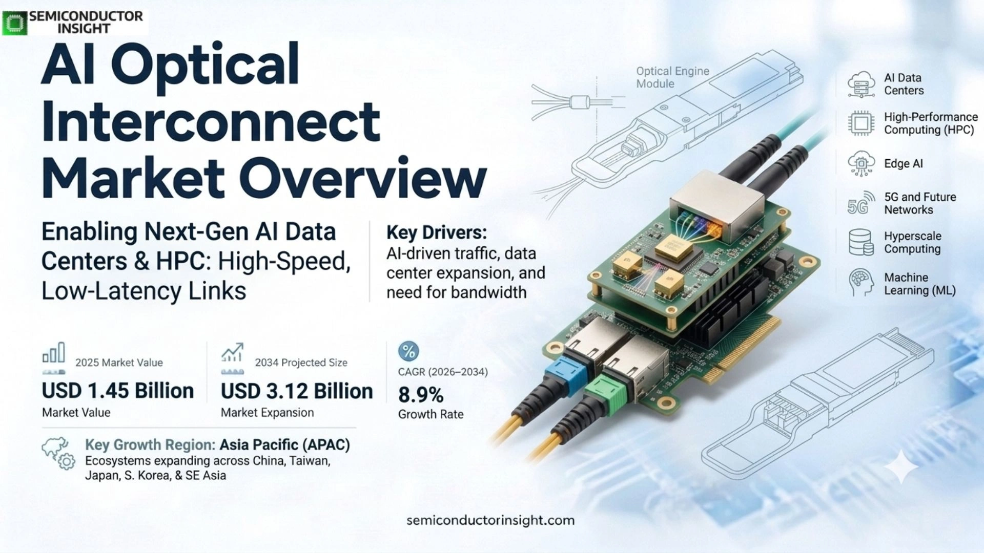
AI Optical Interconnect market was valued at USD 1.45 billion in 2025 and is projected to reach USD 3.12 billion by 2034, representing an 8.9% CAGR during 2026–2034. The 2026 estimated market size is USD 1.58 billion. Asia Pacific is positioned as the largest regional opportunity as cloud, AI and optical-component ecosystems expand across China, Taiwan, Japan, South Korea and Southeast Asia.
AI optical interconnect moves data between accelerators, switches, memory-adjacent systems and racks using photonic links rather than relying exclusively on electrical traces or copper cables. Optical transmission becomes more valuable as link rates rise because electrical loss, equalization power and reach challenges increase rapidly at 200G-per-lane and beyond. The market spans silicon photonic engines, integrated lasers, modulators, detectors, optical fibers, packaging, control ICs and the system architectures that connect them.
The commercial architecture is evolving along a continuum from front-panel pluggable optics toward on-board optics, near-package optics and co-packaged optics. Pluggables remain easy to service and replace, but the electrical path between a switch ASIC and the front panel consumes power and limits future bandwidth density. Moving the optical engine closer to the ASIC shortens the electrical reach, reduces retiming and can improve energy per bit, while introducing new packaging, fiber-attach, thermal and serviceability challenges.
AI clusters create unusually strong east-west traffic because thousands of GPUs or custom accelerators exchange parameters, gradients and inference data continuously. Network performance therefore influences how much of an expensive accelerator fleet is actually utilized. Optical interconnect suppliers compete on bandwidth density, latency, energy per bit, fiber count, laser architecture, yield and field serviceability rather than on optical-module speed alone.
Segment Analysis: By Type
By type, the report segments the market into Silicon Photonic Links, Integrated Laser Modules and Micro-Ring Resonator Solutions. Silicon photonic links lead because they can integrate high-speed optical functions with semiconductor manufacturing flows and support scalable wavelength, modulator and detector architectures for AI switches, optical engines and co-packaged systems.
| Type | Technical role | Market position |
|---|---|---|
| Silicon Photonic Links | Silicon photonics integrates waveguides, modulators, couplers and detectors on semiconductor wafers so optical functions can be produced using highly repeatable lithographic processes. The platform can support wavelength-division multiplexing, high channel counts and close integration with SerDes or switch silicon, making it suitable for dense AI networking. | Leading type. The architecture is central to emerging co-packaged optics and photonic-engine products because it provides a manufacturable path to very high aggregate bandwidth while reducing the electrical distance between the ASIC and the optical conversion point. |
| Integrated Laser Modules | Optical links require stable laser power, delivered either through integrated light sources or external laser systems coupled into photonic engines. Laser modules must provide wavelength control, efficiency, reliability and redundancy across many channels. External-laser approaches can move heat away from the switch package and improve field replacement options. | A strategically important component segment. As CPO scales, laser architecture becomes a system-level decision involving thermal management, fiber routing and serviceability rather than a simple transceiver subcomponent choice. |
| Micro-Ring Resonator Solutions | Micro-ring resonators can modulate or filter specific optical wavelengths in a very small footprint, enabling dense wavelength-division multiplexing and high bandwidth density. Their compact size is attractive for photonic interposers and optical engines, but temperature sensitivity and control complexity require careful design. | A high-value enabling technology within integrated photonics. Suppliers differentiate through thermal stability, tuning efficiency, low insertion loss and co-design with the electrical SerDes and package environment. |
Architecture and deployment-model segmentation
The market also segments by network architecture and deployment model. Multi-stage switch fabrics are important for large distributed AI clusters because they support deterministic high-bandwidth paths across thousands of accelerators. Point-to-point links are simpler for device or rack connections, while reconfigurable meshes can allocate optical paths more dynamically. On-premises, colocation and managed-service deployments have different priorities around capital ownership, serviceability and upgrade cadence.
| Axis | Segments | Commercial implication |
|---|---|---|
| By Architecture | Multi-Stage Switch Fabric · Point-to-Point Links · Reconfigurable Mesh | Multi-stage fabrics dominate large AI clusters where radix and non-blocking bandwidth are critical. Point-to-point links serve direct device and rack connections, while reconfigurable optical meshes can improve utilization when traffic patterns change dynamically. |
| By Deployment Model | On-Premises Data Centers · Co-location Facilities · Managed Services | On-premises hyperscalers can optimize optics tightly with their switch and accelerator architectures, colocation operators prioritize interoperability and maintainability, and managed services favor standardized modules and lifecycle support across multiple customer workloads. |
Segment Analysis: By Application
By application, Data Center Interconnects are the dominant segment, followed by high-performance computing, edge AI accelerators and other uses. AI clusters create sustained high-throughput traffic within and between racks, so optical links are moving deeper into the data center from long-reach network boundaries toward scale-out and scale-up fabrics.
| Application | Demand characteristics |
|---|---|
| Data Center Interconnects | The largest application covers switch-to-switch, rack-to-rack and increasingly package-adjacent optical connectivity inside AI data centers. Operators need to move many terabits per second while keeping network power and latency under control. CPO and near-package optics reduce long electrical traces and can improve bandwidth density, but the architecture must remain installable and serviceable at hyperscale. |
| High-Performance Computing | HPC systems use tightly synchronized networks for scientific simulation, AI research and large-scale modeling. Optical interconnects help extend low-latency fabrics across large machine footprints without the power and reach limits of high-speed copper. Reliability, deterministic latency and error performance are critical because network stalls can reduce utilization across the entire compute job. |
| Edge AI Accelerators | Edge systems need compact, low-power high-speed links when cameras, sensors or local accelerators generate more data than traditional electrical interfaces can move efficiently. Adoption is earlier-stage than in hyperscale data centers because cost and environmental requirements vary widely, but industrial and autonomous systems create a long-term opportunity for smaller optical engines. |
| Others | Telecommunications, storage, disaggregated memory and research systems create additional optical-interconnect demand. Coherent and direct-detect technologies can address different distances, while optical circuit switching and photonic fabrics may become more important as AI infrastructure expands beyond conventional Ethernet and InfiniBand topologies. |
Regional Analysis
Asia Pacific is positioned as the largest and fastest-growing AI Optical Interconnect region, supported by large cloud markets, semiconductor manufacturing, optical-component supply chains and expanding AI data centers. North America remains the strongest technology-development and hyperscale deployment center, while Europe emphasizes energy efficiency, research and sovereign digital infrastructure.
How do regional AI optical-interconnect ecosystems differ?
Optical interconnect is a globally integrated supply chain. North American companies lead much of the switch, accelerator and photonic-system architecture, while Asia Pacific supplies large portions of semiconductor, packaging, laser, module and fiber manufacturing and is building significant AI infrastructure of its own. Europe contributes photonics research, telecom technology and energy-efficient data-center demand, while emerging regions adopt optics primarily through imported AI systems and cloud platforms.
| Region | Market position | Growth outlook | Demand profile | What decides supplier selection |
|---|---|---|---|---|
| Asia Pacific | Largest / fastest-growing outlook | Very high | Cloud, telecom & manufacturing | Scale, manufacturing depth and cost |
| North America | Technology and hyperscale hub | Very high | AI clusters & switch silicon | Bandwidth density, energy per bit and serviceability |
| Europe | Research and efficiency market | High | Cloud, telecom & HPC | Efficiency, interoperability and sovereign infrastructure |
| South America | Emerging | Moderate | Cloud & digital services | Cost, availability and global platform support |
| Middle East & Africa | Early-stage / fast investment | High from small base | Sovereign AI & telecom | Access to current optical networking platforms |
Competitive Landscape
Key participants include Intel, Cisco Systems, NVIDIA, Lumentum, Lightmatter, IBM, Broadcom, Marvell, Axsun Technologies, Ayar Labs, Ciena, Acacia Communications, II-VI and Juniper Networks. The market is shifting from discrete transceiver competition toward system-level photonic integration in which switch silicon, SerDes, lasers, optical engines, fiber attach, advanced packaging and network software are co-designed.
Broadcom has one of the most mature CPO switch positions. Its Tomahawk 6 Davisson integrates co-packaged optics into a 102.4 Tbps Ethernet platform, while the wider portfolio includes SerDes, optical DSP and connectivity devices for scale-up and scale-out AI. The strategy demonstrates how optical interconnect can be sold as part of a complete switch architecture rather than as a separate front-panel transceiver.
NVIDIA is integrating silicon photonics directly into its Quantum InfiniBand and Spectrum-X Ethernet roadmaps. The company positions CPO around 200G SerDes, lower network power, higher resiliency and simplified high-scale deployment. This is strategically important because NVIDIA also controls the accelerators and AI networking software, allowing optical design choices to be optimized across the full compute fabric.
Lightmatter and Ayar Labs represent a newer optical-I/O category focused on moving photonics closer to compute silicon. Lightmatter’s Passage roadmap spans on-board, near-package and 3D co-packaged architectures with very high aggregate bandwidth, while collaborations with GUC, Qualcomm, Synopsys and Cadence aim to create a manufacturable ecosystem. Incumbents such as Cisco/Acacia, Marvell/Inphi, Lumentum and Coherent contribute coherent DSP, lasers and transceiver technology.
Competitive tier structure
| Tier | Companies | Basis of competition |
|---|---|---|
| AI network platform leaders | NVIDIA; Broadcom; Cisco / Acacia; Marvell | Switch ASICs, networking software, SerDes, optical DSP, CPO and large-scale AI fabric integration |
| Photonic engine innovators | Lightmatter; Ayar Labs; Intel silicon photonics; IBM research | Optical I/O, silicon photonics, 3D photonic integration, wavelength multiplexing and package-adjacent optics |
| Optical component & systems suppliers | Lumentum; Coherent (II-VI); Ciena; Juniper; Axsun Technologies | Lasers, components, coherent modules, optical transport and system integration |
Key companies profiled in the report scope
- Intel
- Cisco Systems
- NVIDIA Corporation
- Lumentum Holdings
- Lightmatter
- IBM Corporation
- Broadcom Inc.
- Marvell Technology (Inphi)
- Axsun Technologies
- Ayar Labs
- Ciena Corporation
- Acacia Communications
- II-VI Incorporated / Coherent
- Juniper Networks
AI Optical Interconnect Manufacturing & Deployment Capacity Analysis
Capacity is not defined only by photonic wafer starts. Commercial scaling requires silicon-photonics fabrication, high-speed electrical SerDes, lasers, photonic packaging, fiber-array attachment, optical test and final switch or accelerator integration. A bottleneck in any one of these steps can limit system output, so vendors are building partnerships across foundries, OSATs, ASIC designers and optical-component suppliers.
Silicon-photonics manufacturing can leverage mature semiconductor processes, but photonic yield is influenced by waveguide dimensions, coupler loss, modulator performance and optical alignment. Wafer-level optical test is more complex than conventional electrical probing because light must be coupled into and out of the die. Scaling CPO therefore requires test automation, known-good photonic die and package flows that preserve optical performance through bonding and fiber attach.
Fiber attach and serviceability are becoming important manufacturing constraints. A co-packaged switch may terminate hundreds of fibers near the ASIC, and permanently bonded fiber assemblies can complicate field repair. New detachable fiber-array approaches are designed to separate manufacturing yield from serviceability and allow optical assemblies to be replaced without scrapping the switch ASIC, improving the commercial practicality of very high-bandwidth CPO.
Market Dynamics
Growth is driven by generative-AI traffic, 800G/1.6T networking, switch bandwidth scaling, rising network power and the need to move optics closer to compute. Restraints include manufacturing complexity, laser and packaging cost, serviceability, thermal co-design and fragmented architecture choices. Opportunities are strongest in CPO, optical I/O, DWDM, detachable fiber attach and 200G/400G-per-lane systems.
MARKET DRIVERS
Drivers Impact Analysis*
| Factor | Forecast impact* | Geographic relevance | Impact timeline |
|---|---|---|---|
| AI cluster bandwidth growth | High | North America, Asia Pacific | Short to long term |
| Network power constraints | High | Global hyperscale data centers | Persistent |
| 200G/400G lane scaling | High | Global | Medium term |
| Silicon-photonics manufacturing maturity | Medium to high | North America, Asia Pacific, Europe | Medium term |
*Directional analytical rating; it is not a measured contribution to the headline CAGR.
AI clusters require much more east-west bandwidth
Training and inference systems exchange data continuously across thousands of accelerators. If the network cannot keep pace, expensive GPUs spend time waiting rather than computing. This gives operators a direct economic incentive to adopt higher-radix switches, faster optical links and topologies that maintain low congestion and latency across very large accelerator domains.
Electrical reach becomes more power-intensive at higher speeds
At 200G-per-lane and above, long PCB traces and copper links require strong equalization or retiming. These functions consume power and create heat near already power-dense switch ASICs. Moving optical conversion closer to the silicon shortens the electrical path and can improve energy per bit, making CPO and near-package optics increasingly attractive.
Silicon photonics increases bandwidth density
Photonic integration allows many optical channels and wavelengths to be placed in a small area. DWDM can carry several wavelengths on one fiber, reducing fiber count and connector density as aggregate bandwidth rises. Advances in modulators, resonators, lasers and packaging are therefore expanding the practical ceiling for AI interconnect bandwidth.
System vendors are commercializing CPO
CPO is moving beyond laboratory demonstrations. Broadcom is shipping a 102.4 Tbps optical switch and NVIDIA has introduced silicon-photonics switch platforms for AI networking. Commercial products reduce adoption risk for data-center operators and establish supply chains for optical engines, lasers, fiber attach and field service.
MARKET RESTRAINTS
Restraints Impact Analysis*
| Factor | Forecast impact* | Geographic relevance | Impact timeline |
|---|---|---|---|
| Photonic packaging complexity | High | Global | Persistent |
| Fiber serviceability and field repair | High | Hyperscale deployments | Medium term |
| Laser / thermal management | Medium to high | CPO systems | Persistent |
| Architecture fragmentation | Medium | Global | Short to medium term |
*Directional analytical rating; it is not a measured contribution to the headline CAGR.
Optical packaging has tighter alignment requirements
Photonic chips require precise coupling between waveguides, fibers and laser sources. Small alignment errors can increase insertion loss and reduce link margin. High-volume CPO manufacturing therefore needs advanced packaging, optical metrology and automated assembly that are more specialized than conventional switch or transceiver assembly.
Serviceability is harder when optics are inside the switch
Front-panel pluggable optics can be replaced independently when a module fails. CPO moves the optical engine beside the switch ASIC, potentially making failures more disruptive. Vendors are developing detachable fiber arrays, external lasers and modular optical engines so operators can retain serviceability without giving up the electrical-reach benefits of co-packaging.
Thermal design becomes a shared optical-electrical problem
High-radix switch ASICs dissipate substantial heat, while lasers and resonators can be temperature sensitive. Placing optics near hot silicon requires careful cooling, wavelength control and package materials. External laser sources can reduce local heat but add fiber routing and redundancy complexity.
The industry is still choosing among several integration paths
Pluggable, on-board, near-package and co-packaged optics can all serve AI systems, and the best option depends on reach, power, serviceability and product generation. Customers may delay full CPO adoption until interface standards, field-repair models and multi-vendor supply become clearer.
MARKET OPPORTUNITIES
Scale 102.4T and 200T optical switching
Switch bandwidth is doubling rapidly as AI clusters grow. Broadcom already offers 102.4 Tbps CPO and is demonstrating a broader path toward 200T-class AI infrastructure. Suppliers of photonic engines, lasers, fiber attach and optical test can capture more content as each switch carries hundreds of high-speed optical lanes.
Bring photonics directly to AI accelerators
Optical I/O can move beyond the network switch and connect directly to XPUs, chiplets or photonic interposers. Lightmatter’s 3D Passage platform illustrates this direction. The opportunity is to remove the electrical shoreline bottleneck around large AI dies and create much higher off-package bandwidth density.
Use DWDM to reduce fiber count
Carrying many wavelengths on a single fiber increases bandwidth density without a proportional increase in connectors and cabling. Lightmatter’s 16-wavelength 1.6 Tbps-per-fiber demonstration shows the potential. The commercial challenge is maintaining laser stability, insertion loss and control across a dense wavelength grid.
Standardize detachable and serviceable CPO
Data-center operators need field-replaceable systems. Detachable fiber arrays and modular external laser sources can make CPO easier to deploy and maintain. Vendors that solve serviceability can reduce one of the biggest operational objections to moving optics from the front panel into the switch package.
AI Optical Interconnect Value Chain Analysis
Electrical and optical design must be co-optimized
The optical engine receives high-speed electrical data from a switch or accelerator through SerDes. As lane rates rise, the electrical interface itself can become a power bottleneck. Vendors therefore co-design SerDes reach, modulator drive voltage, photonic architecture and package geometry so that the electrical path is short enough to preserve the efficiency advantage of optics.
Foundry processes determine photonic consistency
Waveguides, modulators, detectors and couplers depend on tightly controlled semiconductor dimensions. Foundries need photonic process design kits and wafer-level test methods in addition to conventional electrical models. Mature silicon-photonics manufacturing can lower cost, but yield must remain high across many optical channels per die.
Packaging connects nanometer-scale photonics to field-serviceable fibers
Photonic engines need precise fiber coupling, laser delivery, thermal control and mechanical protection. Co-packaged systems place these functions close to a large switch ASIC, making package architecture unusually complex. Detachable fiber arrays and standardized optical engines can improve manufacturability and maintenance.
Network economics determine adoption
The final buyer evaluates total cluster performance, not only optical-module cost. A more expensive photonic architecture can be attractive if it reduces network power, avoids GPU idle time or allows a larger non-blocking fabric. This system-level value is why AI workloads are accelerating optical adoption faster than ordinary enterprise networking.
Recent Developments in the AI Optical Interconnect Market
Broadcom showcases 102.4T CPO and 400G/lane optical roadmap
At OFC 2026, Broadcom highlighted a 102.4 Tbps Ethernet switch with co-packaged optics, 400G-per-lane optical DSP and related AI connectivity products. The portfolio shows optical and electrical interconnect being designed together for gigawatt-scale AI clusters.
Lightmatter demonstrates 1.6 Tbps per fiber
Lightmatter sampled a Passage CPO chiplet using 16-wavelength DWDM and 112G SerDes to reach 1.6 Tbps per fiber. The design targets much higher bandwidth density for AI interconnect while reducing the number of physical fibers required.
Lightmatter introduces 6.4 Tbps-per-direction L20 optical engine
The Passage L20 supports near-package and on-board optics and uses bidirectional multiplexing to increase fiber bandwidth density. The product broadens the deployment path between traditional pluggables and full 3D co-packaged optics.
Broadcom ships 102.4 Tbps Tomahawk 6 Davisson CPO switch
Broadcom announced shipment of its third-generation CPO Ethernet switch, integrating 102.4 Tbps of optical switching capacity for AI scale-up and scale-out networks. Commercial shipment is a major step in moving CPO from demonstration to production infrastructure.
Lightmatter unveils Passage M1000 photonic superchip
Lightmatter announced a 3D photonic interposer reference platform with up to 114 Tbps of optical bandwidth and a package area above 4,000 square millimeters, targeting very large multi-die AI systems.
REPORT SCOPE & SEGMENTATION
| Attribute | Details |
|---|---|
| Study Period | 2021–2034 |
| Base Year | 2025 |
| Estimated Year | 2026 |
| Forecast Period | 2026–2034 |
| Historical Period | 2021–2025 |
| Market Size 2025 | USD 1.45 billion |
| Market Size 2034 | USD 3.12 billion |
| Growth Rate | CAGR of 8.9% from 2026–2034 |
| Unit | Value (USD Million/Billion) and optical-link / module shipments where applicable |
| Segmentation | By Type, By Application, By End User, By Architecture, By Deployment Model, By Region |
| By Type | Silicon Photonic Links · Integrated Laser Modules · Micro-Ring Resonator Solutions |
| By Application | Data Center Interconnects · High-Performance Computing · Edge AI Accelerators · Others |
| By End User | Hyperscale Cloud Providers · Telecommunications Operators · Enterprise AI Labs |
| By Architecture | Multi-Stage Switch Fabric · Point-to-Point Links · Reconfigurable Mesh |
| By Deployment Model | On-Premises Data Centers · Co-location Facilities · Managed Services |
| By Region | Each region analysed by interconnect type, application, end user, network architecture, deployment model and country ecosystemNorth AmericaUnited States, Canada, MexicoEuropeGermany, France, United Kingdom, Netherlands, Belgium and other European marketsAsia PacificChina, Taiwan, Japan, South Korea, India, Southeast Asia and other Asian marketsSouth AmericaBrazil, Chile, Argentina and other South American marketsMiddle East & AfricaSaudi Arabia, UAE, Israel, South Africa and other MEA markets |
| Key Companies Profiled | Intel · Cisco Systems · NVIDIA Corporation · Lumentum Holdings · Lightmatter · IBM Corporation · Broadcom Inc. · Marvell Technology (Inphi) · Axsun Technologies · Ayar Labs · Ciena Corporation · Acacia Communications · II-VI Incorporated / Coherent · Juniper Networks |
| Customization Scope | Free report customization equivalent to up to four analyst working days with purchase. Addition or alteration to country, regional and segment scope. |
Frequently Asked Questions
What is the 2025 size of the AI Optical Interconnect market?
The market was valued at USD 1.45 billion in 2025 and is projected to reach USD 3.12 billion by 2034. The 2026 estimated market size is USD 1.58 billion and the 2026–2034 growth rate is 8.9%, reflecting continued expansion of optical connectivity inside AI and high-performance computing infrastructure.
Which AI optical interconnect type leads the market?
Silicon photonic links lead because they provide a scalable semiconductor-manufacturing path for modulators, waveguides and detectors and can support dense wavelength multiplexing. The technology is central to on-board, near-package and co-packaged optical engines where bandwidth density and energy per bit are more important than conventional front-panel module simplicity.
Which application is the largest?
Data center interconnects are the largest application because AI training and inference clusters exchange enormous data volumes between accelerators and switches. Optical links are increasingly used inside the data center rather than only between facilities, and higher switch speeds are pushing optical conversion closer to the networking ASIC.
Which region leads the growth outlook?
Asia Pacific is positioned as the largest and fastest-growing regional opportunity, supported by cloud infrastructure, telecom networks, semiconductor manufacturing and optical-component supply chains. North America remains the primary technology-development and hyperscale deployment hub through companies such as NVIDIA, Broadcom, Cisco, Marvell, Lightmatter and major cloud operators.
What is the estimated market size in 2026?
The 2026 estimated market size is USD 1.58 billion. This value is consistent with the 2025 base of USD 1.45 billion and the 2034 forecast of USD 3.12 billion, which together correspond to an 8.9% growth path through the forecast period.
Why is co-packaged optics important for AI?
CPO moves optical engines beside the switch or compute ASIC, shortening the high-speed electrical path that otherwise requires power-hungry SerDes equalization and retiming. The architecture can improve bandwidth density and energy per bit, which becomes increasingly valuable as AI switches reach 102.4 Tbps and future systems target even higher aggregate bandwidth.
What are the main market restraints?
The main restraints are photonic packaging complexity, precise fiber alignment, laser and thermal management, serviceability and uncertainty over the timing of pluggable, on-board, near-package and CPO adoption. Customers also need multi-vendor supply and proven field reliability before moving critical AI networks to new architectures at large scale.
What recent technology milestone is most important?
Commercial 102.4 Tbps CPO switching and 1.6 Tbps-per-fiber demonstrations are two important milestones. Broadcom is shipping a 102.4 Tbps optical Ethernet switch, while Lightmatter has demonstrated dense 16-wavelength optical transmission at 1.6 Tbps per fiber and introduced optical engines for several packaging positions.
How does optical interconnect improve AI cluster economics?
Optical interconnect can reduce network power and enable larger high-bandwidth fabrics, improving accelerator utilization. When GPUs cost far more than the network links that connect them, preventing idle time can justify higher-value optical infrastructure. Lower electrical reach also helps reduce retiming power and cooling demand as link rates increase.
What does the report cover?
The report covers silicon photonic links, integrated laser modules and micro-ring resonator solutions; data center, HPC, edge AI and other applications; hyperscale, telecom and enterprise AI end users; multi-stage, point-to-point and mesh architectures; deployment models; five global regions; manufacturing analysis; and the full profiled company set.
Research Sources & Evidence Base
View primary and authoritative evidence used in this overview
- NVIDIA. Silicon Photonics Networking for Agentic AI – Official product information on CPO-based Spectrum-X and Quantum networking, 200G SerDes, power efficiency and large-scale AI fabrics.
- Broadcom. OFC 2026 AI Infrastructure Portfolio – Official March 2026 announcement covering 102.4T CPO switching, 400G/lane optical DSP and related AI interconnect products.
- Broadcom. Tomahawk 6 Davisson 102.4T CPO Switch – Official October 2025 shipment announcement for third-generation co-packaged optical Ethernet switching.
- Lightmatter. 1.6 Tbps per Fiber CPO Milestone – March 2026 primary evidence on 16-wavelength DWDM and high-bandwidth photonic interconnect sampling.
- Lightmatter. Passage L20 Optical Engine – March 2026 product evidence on 6.4 Tbps-per-direction optical engines for NPO and OBO architectures.
- Lightmatter. Passage M1000 Photonic Superchip – March 2025 evidence on 3D photonic interposer scaling and 114 Tbps aggregate optical bandwidth.

Get Sample Report PDF for Exclusive Insights
Report Sample Includes
- Table of Contents
- List of Tables & Figures
- Charts, Research Methodology, and more...
 Download Sample Report PDF



