AI Low-alpha Solder Bump Material Radioactivity Screening Processor Market Insights
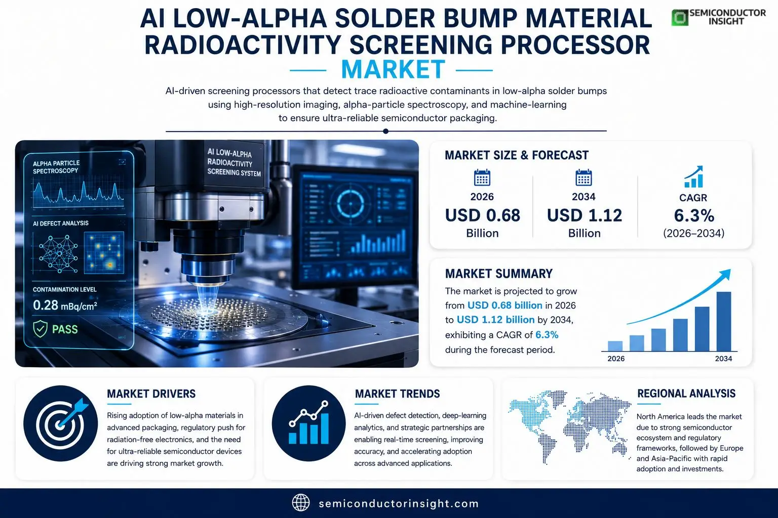
AI Low-alpha Solder Bump Material Radioactivity Screening Processor market size was valued at USD 0.62 billion in 2025. The market is projected to grow from USD 0.68 billion in 2026 to USD 1.12 billion by 2034, exhibiting a CAGR of 6.3% during the forecast period.
AI Low-alpha solder bump material radioactivity screening processors are specialized inspection systems designed to detect trace radioactive contaminants in low‑alpha solder bumps used in advanced semiconductor packaging. These processors combine high‑resolution imaging, machine‑learning algorithms, and alpha‑particle spectroscopy to ensure compliance with stringent reliability standards for aerospace, defense, and high‑performance computing applications.The market is experiencing rapid growth because demand for ultra‑reliable semiconductor devices is rising, regulatory scrutiny on radioactive contamination is tightening, and AI‑driven defect detection technologies are advancing. Furthermore, major semiconductor manufacturers are investing heavily in next‑generation packaging solutions that require precise low‑alpha material verification. Recent collaborationssuch as the March 2024 partnership between NanoTech Instruments and Advanced Materials Corp., which integrates deep‑learning analytics into radioactivity screening workflowsillustrate the momentum propelling this niche yet critical segment.
MARKET DRIVERS
Rising Adoption of Low‑Alpha Materials in Advanced Packaging
Manufacturers of high‑performance semiconductors are increasingly selecting AI Low-alpha Solder Bump Material Radioactivity Screening Processor Market solutions to meet strict defect‑density targets. The move toward 5‑nm and finer nodes heightens sensitivity to alpha particle contamination, driving demand for reliable screening technologies.
Regulatory Push for Radiation‑Free Electronics
safety standards now mandate verification of radioactivity levels in solder bump materials, especially for aerospace and medical devices. Companies that integrate AI‑enabled screening processors gain a competitive edge by ensuring compliance while reducing rework cycles.
➤ “The ability to detect sub‑ppm alpha emissions in real‑time has become a decisive factor for tier‑1 suppliers.”
Overall, the convergence of technology scaling, regulatory scrutiny, and cost‑avoidance strategies creates a robust growth engine for AI Low-alpha Solder Bump Material Radioactivity Screening Processor Market.
MARKET CHALLENGES
High Capital Expenditure for Advanced Screening Equipment
Deploying AI‑driven radioactivity screening systems requires significant upfront investment in precision instrumentation and data‑analytics infrastructure. Smaller fab operators often face budget constraints that delay adoption.
Other Challenges
Integration Complexity
Seamlessly embedding screening processors into existing production lines demands specialized engineering expertise, and any integration mishap can lead to yield losses.
MARKET RESTRAINTS
Limited Availability of Skilled AI Talent
The effectiveness of AI Low-alpha Solder Bump Material Radioactivity Screening Processor Market solutions hinges on skilled data scientists and engineers. A shortage of qualified professionals slows implementation and hampers performance optimization.
MARKET OPPORTUNITIES
Emergence of Edge‑AI Analytics for In‑Line Monitoring
Advances in edge‑AI enable real‑time analysis of alpha‑particle data directly on the production floor, reducing latency and improving decision‑making. Companies that adopt these capabilities can unlock higher throughput and lower defect rates in AI Low-alpha Solder Bump Material Radioactivity Screening Processor Market.
AI Low-alpha Solder Bump Material Radioactivity Screening Processor Market Trends
Rising Demand for Ultra‑Reliable Semiconductor Packaging
AI Low-alpha Solder Bump Material Radioactivity Screening Processor Market is being reshaped by a growing need for ultra‑reliable semiconductor devices across aerospace, defense, and high‑performance computing sectors. As manufacturers pursue finer geometries and advanced 3D‑IC configurations, the tolerance for radioactive contamination in low‑alpha solder bumps narrows dramatically. Regulatory bodies are tightening inspection requirements, prompting production lines to adopt specialized screening processors that combine high‑resolution imaging with machine‑learning‑driven analysis. This convergence of stringent standards and technological capability is driving a clear shift toward integrated, AI‑enhanced solutions that can detect trace alpha particles in real time, reducing warranty costs and enhancing product lifespan.
Other Trends
Strategic Partnerships Accelerating Technology Integration
Recent strategic collaborations illustrate the momentum behind the segment. In March 2024, NanoTech Instruments partnered with Advanced Materials Corp. to embed deep‑learning analytics directly into radioactivity screening workflows. The joint effort enables predictive defect classification, allowing engineers to intervene before contamination propagates through the assembly process. Similar alliances are emerging between equipment manufacturers and AI software firms, creating a pipeline of turnkey solutions that reduce operator dependence and improve throughput. These partnerships not only shorten development cycles but also standardize best‑practice methodologies, fostering broader industry adoption of low‑alpha verification technologies.
AI‑Driven Defect Detection as a Competitive Differentiator
Beyond compliance, AI‑driven defect detection is becoming a competitive differentiator for semiconductor suppliers. By leveraging alpha‑particle spectroscopy data alongside convolutional neural networks, processors can identify subtle contamination patterns that traditional methods miss. This heightened sensitivity supports the production of next‑generation packaging formats such as integrated fan‑out wafer‑level chip‑scale packages, where even minimal radioactive exposure can compromise performance under extreme conditions. Companies that integrate these advanced screening processors report higher yield rates and lower scrap ratios, reinforcing their market position and attracting customers seeking assurance of long‑term reliability. As the ecosystem matures, continuous algorithm refinement and sensor miniaturization are expected to further embed AI Low‑alpha screening capabilities into standard manufacturing lines.
COMPETITIVE LANDSCAPEKey Industry Players
Competitive Overview of AI Low‑alpha Solder Bump Material Radioactivity Screening Processors
The AI Low‑alpha Solder Bump Material Radioactivity Screening Processor market is currently dominated by a small cohort of technology‑focused firms that combine advanced spectroscopy with AI‑driven defect analytics. NanoTech Instruments, leveraged by its 2024 partnership with Advanced Materials Corp., is widely recognized as the market leader due to its integrated deep‑learning platform that reduces inspection cycle time by up to 30 %. KLA Corporation follows closely, offering a high‑throughput imaging suite that is favoured by major aerospace and defense chip manufacturers. Both companies benefit from the market’s robust CAGR of 6.3 % and the rising regulatory scrutiny on trace radioactive contaminants, positioning them to capture the majority of the projected USD 1.12 billion market size by 2034.Beyond the dominant players, a range of niche specialists are expanding the competitive landscape. ASML’s optical metrology division has entered the space with a hybrid scanner that targets low‑alpha verification for next‑generation 3D‑IC packaging. Teradyne and Advantest contribute dedicated test‑equipment platforms that incorporate alpha‑particle spectroscopy modules. Regional firms such as MKS Instruments, Camtek, and Oxford Instruments bring focused expertise in sensor integration and materials handling, while broader semiconductor equipment suppliers like Applied Materials and Lam Research are developing add‑on kits to complement their existing wafer‑processing portfolios. This diversification of capabilities creates a layered market structure where large incumbents dominate high‑volume contracts and specialized vendors capture high‑margin, application‑specific projects.
List of Key AI Low-alpha Solder Bump Material Radioactivity Screening Processor Companies Profiled
- NanoTech Instruments
- KLA Corporation
- Advanced Materials Corp.
- ASML
- Teradyne
- Advantest
- MKS Instruments
- Camtek
- Oxford Instruments
- Applied Materials
- Lam Research
- Thermo Fisher Scientific
- Hitachi High‑Technologies
- Bruker Corporation
- NXP Semiconductors
Segment Analysis:
| Segment Category | Sub-Segments | Key Insights |
| By Type |
|
Low‑alpha Solder Bump Material is the dominant type because:
|
| By Application |
|
Aerospace and Defense leads application usage because:
|
| By End User |
|
Semiconductor Foundries dominate end‑user demand because:
|
| By Technology |
|
Machine‑Learning Analytics is the pivotal technology because:
|
| By Compliance Requirement |
|
NASA Contamination Standards drive market focus because:
|
Regional Analysis: AI Low-alpha Solder Bump Material Radioactivity Screening Processor Market
North America
The United States continues to pioneer integrated AI workflows, pairing high‑resolution detectors with deep‑learning models that predict contaminant signatures. Industry consortia are standardizing data formats, which accelerates deployment across multinationals and reduces integration costs for niche players.
Canadian firms benefit from government‑backed R&D incentives that target low‑alpha material research. Partnerships between Ottawa‑based startups and established fabs foster rapid prototyping of AI screening modules tailored for mixed‑signal environments.
Mexico’s emerging semiconductor parks attract investment in AI‑enabled inspection lines. Early adopters are focusing on cost‑effective sensor arrays integrated with pretrained models to meet growing regional demand.
Edge‑AI processors and hybrid quantum‑classical algorithms are beginning to appear in pilot projects, promising to enhance detection limits while maintaining real‑time processing capabilities.
Europe
European manufacturers emphasize compliance with strict RoHS and REACH directives, driving the adoption of AI screening tools that can verify low‑alpha content without extensive manual sampling. Collaborative research hubs in Germany and the Netherlands are developing open‑source AI frameworks that enable smaller firms to access sophisticated analytics. The region’s focus on sustainability also encourages the use of predictive maintenance, reducing waste associated with over‑inspection. As a result, Europe is building a balanced market where high‑precision equipment coexists with cost‑effective AI services, fostering widespread confidence in low‑alpha material handling.
Asia‑Pacific
Asia‑Pacific sees rapid expansion of fab capacity in China, Taiwan, and South Korea, where the pressure to meet high‑volume production schedules fuels interest in AI‑driven screening. Companies prioritize scalable cloud platforms that can process large datasets from multiple lines simultaneously. While regulatory frameworks vary, many Asian governments are issuing incentives for AI integration in semiconductor supply chains, encouraging the deployment of low‑alpha detection systems that can be retrofitted to legacy equipment. The resulting ecosystem blends cutting‑edge research with pragmatic, volume‑oriented solutions.
South America
In South America, emerging semiconductor initiatives in Brazil and Argentina are still in early stages, yet they recognize the strategic advantage of AI screening for low‑alpha materials. Regional partnerships with North American vendors provide access to turnkey AI platforms, while local universities contribute research on material purity specific to indigenous supply chains. The market remains niche but is poised for growth as government programs aim to diversify high‑tech manufacturing capabilities.
Middle East & Africa
The Middle East & Africa region is gradually entering the AI screening space, driven by investment in high‑tech parks in the United Arab Emirates and South Africa’s expanding R&D corridors. Stakeholders focus on building foundational data repositories that can train AI models for low‑alpha detection, often leveraging partnerships with European research institutes. Though adoption rates are modest, strategic emphasis on technology transfer and skill development suggests a steady trajectory toward broader market participation.
Report Scope
This market research report provides a comprehensive analysis of the AI Low-alpha Solder Bump Material Radioactivity Screening Processor Market , covering the forecast period 2026–2034. It offers detailed insights into market dynamics, technological advancements, competitive landscape, and key trends shaping the industry.
Key focus areas of the report include:
- Market Overview: The report begins with an overview outlining its current market scenario, key growth indicators, and industry transformation drivers. It discusses macroeconomic factors, demand–supply balance, regulatory landscape, and the strategic role of semiconductors in powering advancements across industries such as automotive, telecommunications, consumer electronics, and industrial automation.
- Market Size & Forecast: Historical data and future projections for revenue, unit shipments, and market value across major regions and segments.
- Segmentation Analysis: Detailed breakdown by product type, technology, application, and end-user industry to identify high-growth segments and investment opportunities.
- Regional Insights: Insights into market performance across North America, Europe, Asia-Pacific, Latin America, and the Middle East & Africa, including country-level analysis where relevant.
- Competitive Landscape: Profiles of leading market participants, including their product offerings, R&D focus, manufacturing capacity, pricing strategies, and recent developments such as mergers, acquisitions, and partnerships.
- Technology Trends & Innovation: Assessment of emerging technologies, integration of AI/IoT, semiconductor design trends, fabrication techniques, and evolving industry standards.
- Market Drivers & Restraints: Evaluation of factors driving market growth along with challenges, supply chain constraints, regulatory issues, and market-entry barriers.
- Stakeholder Insights: Insights for component suppliers, OEMs, system integrators, investors, and policymakers regarding the evolving ecosystem and strategic opportunities.
Primary and secondary research methods are employed, including interviews with industry experts, data from verified sources, and real-time market intelligence to ensure the accuracy and reliability of the insights presented.
FREQUENTLY ASKED QUESTIONS:
What is the current market size of AI Low-alpha Solder Bump Material Radioactivity Screening Processor Market?
-> AI Low-alpha Solder Bump Material Radioactivity Screening Processor Market was valued at USD 0.62 billion in 2025 and is expected to reach USD 1.12 billion by 2034.
Which key companies operate in AI Low-alpha Solder Bump Material Radioactivity Screening Processor Market?
-> Key players include NanoTech Instruments, Advanced Materials Corp., and other leading semiconductor equipment manufacturers.
What are the key growth drivers?
-> Key growth drivers include rising demand for ultra‑reliable semiconductor devices, tightening regulatory scrutiny on radioactive contamination, and advances in AI‑driven defect detection technologies.
Which region dominates the market?
-> North America currently holds a leading share, with strong contributions from Europe and Asia‑Pacific.
What are the emerging trends?
-> Emerging trends include integration of deep‑learning analytics into screening workflows, AI‑enhanced imaging, and development of next‑generation low‑alpha packaging verification solutions.
Get Sample Report PDF for Exclusive Insights
Report Sample Includes
- Table of Contents
- List of Tables & Figures
- Charts, Research Methodology, and more...


