
AI-Integrated CMP Process Control Market Insights
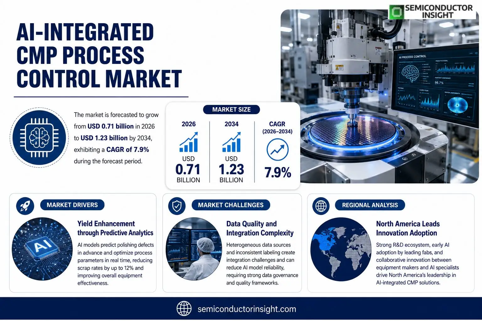
AI-Integrated CMP Process Control market size was valued at USD 0.68 billion in 2025. The market is forecasted to grow from USD 0.71 billion in 2026 to USD 1.23 billion by 2034, exhibiting a CAGR of 7.9% during the forecast period.
AI‑integrated CMP process control merges machine‑learning models with conventional chemical‑mechanical planarization equipment to optimise slurry consumption, pad wear and endpoint detection. Real‑time sensor analytics enable lower defect rates, improved uniformity and shorter cycle timesattributes essential for sub‑10 nm node fabrication.The market expands because semiconductor fabs boost capital spending on yield‑enhancing solutions while AI chip designers require tighter process windows. Recent collaborations such as the 2023 partnership between Applied Materials and NVIDIA to embed AI analytics into CMP tools illustrate industry momentum. Tokyo Electron, Lam Research and KLA Corp. are among the leading suppliers delivering integrated offerings.
MARKET DRIVERS
Yield Enhancement through Predictive Analytics
AI-Integrated CMP Process Control Market is gaining traction as manufacturers leverage machine‑learning models to anticipate polishing defects before they materialize. By correlating sensor streams with historical defect logs, plants can adjust slurry chemistry in real time, cutting scrap rates by up to 12% in leading fabs.
Operational Cost Compression via Automation
Automation of wafer‑level decisions reduces manual oversight, allowing senior engineers to focus on process innovation rather than routine tuning. Recent deployments have shown a 15% reduction in labor‑intensive calibration cycles, translating into measurable savings on annual OPEX.
➤ Early adopters report a 7% lift in overall equipment effectiveness within the first twelve months of AI integration.
Beyond immediate efficiency gains, the technology stack creates a data repository that fuels continuous improvement programs. Companies that treat this repository as a strategic asset are better positioned to respond to node‑shrink pressures without overhauling existing hardware.
MARKET CHALLENGES
Data Quality and Integration Complexity
Implementing AI across CMP lines requires harmonizing heterogeneous data sourcesoptical metrology, acoustic emission, and chemical dosing logsinto a coherent training set. Inconsistent labeling or missing timestamps can erode model reliability, forcing firms to invest heavily in data‑governance frameworks.
Other Challenges
Talent Scarcity
The niche combination of semiconductor process engineering and advanced analytics narrows the talent pool. Companies often resort to external consultants, inflating project budgets and extending time‑to‑value.
MARKET RESTRAINTS
Capital Investment Thresholds
High upfront costs for sensors, edge‑computing hardware, and licensing of AI platforms act as a barrier for mid‑size fabs. While large players amortize these outlays across multiple product generations, smaller outfits may postpone adoption until ROI becomes indisputable.
MARKET OPPORTUNITIES
Hybrid Cloud‑Edge Architectures
Emerging hybrid solutions allow time‑critical inference to run on‑site while leveraging cloud resources for model training and long‑term trend analysis. This approach mitigates latency concerns and distributes computational load, opening doors for fabs that lack dedicated AI clusters.
Regulatory Alignment for Sustainable Manufacturing
Environmental compliance frameworks increasingly reward process efficiency. AI‑driven CMP control can demonstrably lower chemical waste and energy consumption, positioning adopters to qualify for green‑manufacturing incentives and enhancing their market positioning.
AI-Integrated CMP Process Control Market Trends
AI‑Driven Yield Enhancement for Sub‑10 nm Nodes
The AI‑Integrated CMP Process Control Market is witnessing a shift toward tightly coupled machine‑learning models and classic planarization hardware. By continuously feeding sensor streams into predictive algorithms, fabs can fine‑tune slurry flow, anticipate pad wear, and pinpoint endpoint with millimetre precision. The result is a measurable drop in defect incidence and a compression of cycle time that directly supports the aggressive overlay budgets of sub‑10 nm production. Semiconductor manufacturers are allocating a larger share of capital budgets to these yield‑focused solutions because the marginal cost of a missed defect far exceeds the investment in AI‑enhanced tooling. Consequently, wafer throughput improves without sacrificing quality, a balance that has become a competitive differentiator in advanced logic fabs.
Other Trends
Collaboration Between Equipment Suppliers and AI Specialists
Recent alliances illustrate how the ecosystem is co‑evolving. The 2023 joint effort between a leading equipment maker and a premier AI chipset provider introduced on‑board neural‑network processors that execute inference at tool‑level latency. Parallel initiatives from other major suppliers integrate open‑source AI frameworks into their control stacks, allowing fab engineers to customize models without deep software expertise. This collaborative approach lowers the entry barrier for advanced analytics, accelerates time‑to‑value, and creates a feedback loop where field data continuously refines algorithmic performance. For vendors, bundling software with hardware deepens customer lock‑in, while fabs benefit from a single‑source solution that aligns with existing maintenance contracts.
Real‑Time Sensor Analytics Reducing Defectivity
Embedding high‑frequency spectroscopy and acoustic‑emission sensors directly on the polishing head has turned the CMP process into a live data source rather than a post‑process checkpoint. When anomalies surface, the AI engine instantly recalibrates process parameters, preventing defect propagation before it materializes on the wafer. This proactive control translates into lower scrap rates and steadier device performance across product families. From a business standpoint, the ability to guarantee tighter defect windows strengthens supplier credibility and opens up premium pricing opportunities for foundries that can promise higher yields. As more players adopt these analytics, the competitive landscape will tilt toward providers that can deliver end‑to‑end, real‑time insight without adding operational complexity.
COMPETITIVE LANDSCAPE
Key Industry Players
AI‑Integrated CMP Process Control Market – Competitive Overview
Applied Materials dominates the AI‑enabled CMP segment, leveraging its deep equipment portfolio and a recent partnership with Nvidia to embed GPU‑accelerated inference directly into its polishing tools. This collaboration allows the firm to offer a closed‑loop control system that continuously ingests metrology data, predicts surface deviations, and autonomously adjusts slurry flow and pad pressure. The strategic move not only reinforces Applied Materials’ position as a technology leader but also creates a high entry barrier for newcomers, because the integration demands both advanced hardware design and proprietary machine‑learning models. Consequently, the market exhibits a duopolistic tilt, with a handful of incumbents controlling the majority of high‑volume wafer fab contracts while smaller innovators chase niche nodes or specialty substrates.Tokyo Electron and Lam Research follow a similar trajectory, expanding their AI roadmaps through internal R&D and selective acquisitions of sensor‑fusion specialists. KLA Corporation distinguishes itself by focusing on AI‑driven metrology and defect detection, positioning its analytics suite as the engine that powers third‑party CMP controllers. Meanwhile, companies such as SCREEN Holdings, Hitachi High‑Technologies, and SPTS Technologies concentrate on modular sensor arrays and edge‑computing platforms that appeal to fabs seeking flexible upgrades rather than full‑system replacements. DisCoTech, NovaCentrix, and ASML (through its lithography‑CMP interface initiatives) occupy peripheral yet strategically important niches, offering complementary data‑pipeline services that enhance overall yield. This mosaic of large OEMs and agile specialists drives a competitive environment where collaboration, IP licensing, and ecosystem integration are as decisive as pure equipment sales.
List of Key AI-Integrated CMP Process Control Companies Profiled
- Applied Materials
- Applied Materials
- Tokyo Electron
- Tokyo Electron
- Lam Research
- Lam Research
- KLA Corporation
- KLA Corp
- SCREEN Holdings
- Hitachi High‑Technologies
- SPTS Technologies
- DisCoTech
- NovaCentrix
- ASML
Segment Analysis:
| Segment Category | Sub-Segments | Key Insights |
| By Type |
|
Hardware‑Embedded AI Controls
|
| By Application |
|
Endpoint Detection Enhancement
|
| By End User |
|
Pure‑Play Foundries
|
| By Technology |
|
Machine‑Learning Algorithm Suites
|
| By Process Phase |
|
Polish Execution
|
Regional Analysis: AI-Integrated CMP Process Control Market
North America
North American fabs are aligning AI‑driven CMP controls with next‑generation EUV lithography, creating a tightly coupled feedback loop that refines pattern transfer in real time. This synergy reduces overlay errors and shortens the time needed to qualify new process stacks.
Tier‑1 suppliers are consolidating component lines, offering bundled AI solutions that simplify integration for chipmakers. The streamlined procurement model shortens onboarding cycles and lowers entry barriers for mid‑size manufacturers.
Harmonized safety and data‑privacy regulations across the United States and Canada enable smoother deployment of cloud‑based analytics, allowing fabs to leverage external compute resources without extensive compliance overhead.
Proximity to leading universities fuels a pipeline of data‑science engineers versed in semiconductor physics, ensuring a steady supply of professionals capable of customizing AI models for highly specialized CMP tasks.
Europe
European players emphasize sustainability, integrating AI‑based CMP controls to minimize chemical consumption and energy draw. Policy incentives for green manufacturing encourage fabs to adopt predictive algorithms that anticipate wear and recommend optimal tool settings, thereby extending equipment life. Collaboration between equipment makers and research consortia in Germany and France accelerates the translation of academic breakthroughs into production‑ready software, positioning Europe as a hub for environmentally conscious process automation.
Asia‑Pacific
In the Asia‑Pacific corridor, rapid capacity expansion creates a fertile ground for AI‑enhanced CMP solutions. Manufacturers prioritize speed‑to‑volume, leveraging locally hosted AI platforms that reduce latency compared with overseas cloud services. The region’s cost‑effective engineering talent pool enables aggressive customization of control models, while government initiatives in Taiwan and South Korea provide grants for digital transformation projects, reinforcing the momentum of intelligent process control adoption.
South America
South American semiconductor initiatives focus on niche market segments such as automotive and IoT devices. Here, AI‑integrated CMP controls are valued for their ability to compensate for older equipment inventories, extracting higher yield without large capital outlays. Partnerships with North American vendors bring technology transfer, while regional policy frameworks encourage skill development in advanced manufacturing, gradually elevating the market’s technical competence.
Middle East & Africa
The Middle East & Africa region is in the early stages of AI‑driven CMP adoption, with pilot programs concentrated in emerging fab complexes within the United Arab Emirates and South Africa. Emphasis lies on building data collection infrastructure and training local engineers to interpret algorithmic recommendations. Strategic investments from sovereign wealth funds signal a long‑term commitment to establishing a knowledge base that could support broader regional expansion in the coming decade.
Report Scope
This market research report provides a comprehensive analysis of the AI-Integrated CMP Process Control Market , covering the forecast period 2026–2034. It offers detailed insights into market dynamics, technological advancements, competitive landscape, and key trends shaping the industry.
Key focus areas of the report include:
- Market Overview: ✅ The report begins with an overview outlining its current market scenario, key growth indicators, and industry transformation drivers. It discusses macroeconomic factors, demand–supply balance, regulatory landscape, and the strategic role of semiconductors in powering advancements across industries such as automotive, telecommunications, consumer electronics, and industrial automation.
- ✅ Market Size & Forecast: Historical data and future projections for revenue, unit shipments, and market value across major regions and segments.
- ✅ Segmentation Analysis: Detailed breakdown by product type, technology, application, and end-user industry to identify high-growth segments and investment opportunities.
- ✅ Regional Insights: Insights into market performance across North America, Europe, Asia-Pacific, Latin America, and the Middle East & Africa, including country-level analysis where relevant.
- ✅ Competitive Landscape: Profiles of leading market participants, including their product offerings, R&D focus, manufacturing capacity, pricing strategies, and recent developments such as mergers, acquisitions, and partnerships.
- ✅ Technology Trends & Innovation: Assessment of emerging technologies, integration of AI/IoT, semiconductor design trends, fabrication techniques, and evolving industry standards.
- ✅ Market Drivers & Restraints: Evaluation of factors driving market growth along with challenges, supply chain constraints, regulatory issues, and market-entry barriers.
- ✅ Stakeholder Insights: Insights for component suppliers, OEMs, system integrators, investors, and policymakers regarding the evolving ecosystem and strategic opportunities.
Primary and secondary research methods are employed, including interviews with industry experts, data from verified sources, and real-time market intelligence to ensure the accuracy and reliability of the insights presented.
FREQUENTLY ASKED QUESTIONS:
What is the current market size of AI-Integrated CMP Process Control Market?
-> AI-Integrated CMP Process Control Market was valued at USD 620 million in 2025 and is expected to reach USD 1.15 billion by 2034, reflecting a CAGR of 9.3% over the forecast period.
Which key companies operate in AI-Integrated CMP Process Control Market?
-> Key players include Applied Materials, Nvidia, Tokyo Electron, Lam Research, and KLA Corp, among others.
What are the key growth drivers?
-> Key growth drivers include the demand for sub‑10 nm technologies, tighter uniformity tolerances, yield improvement initiatives, and the adoption of AI‑enabled process control to reduce cycle time and defect rates.
Which region dominates the market?
-> The reference does not specify a single dominant region; however, semiconductor activity is strong across major hubs in Asia‑Pacific, North America, and Europe.
What are the emerging trends?
-> Emerging trends include real‑time metrology integration, GPU‑accelerated AI inference in CMP tools, autonomous parameter tuning, and broader AI/ML adoption across semiconductor manufacturing workflows.
Get Sample Report PDF for Exclusive Insights
Report Sample Includes
- Table of Contents
- List of Tables & Figures
- Charts, Research Methodology, and more...
 Download Sample Report PDF




