
AI for Known Good Die Screening in Multi-Chip Module Assembly Market Insights
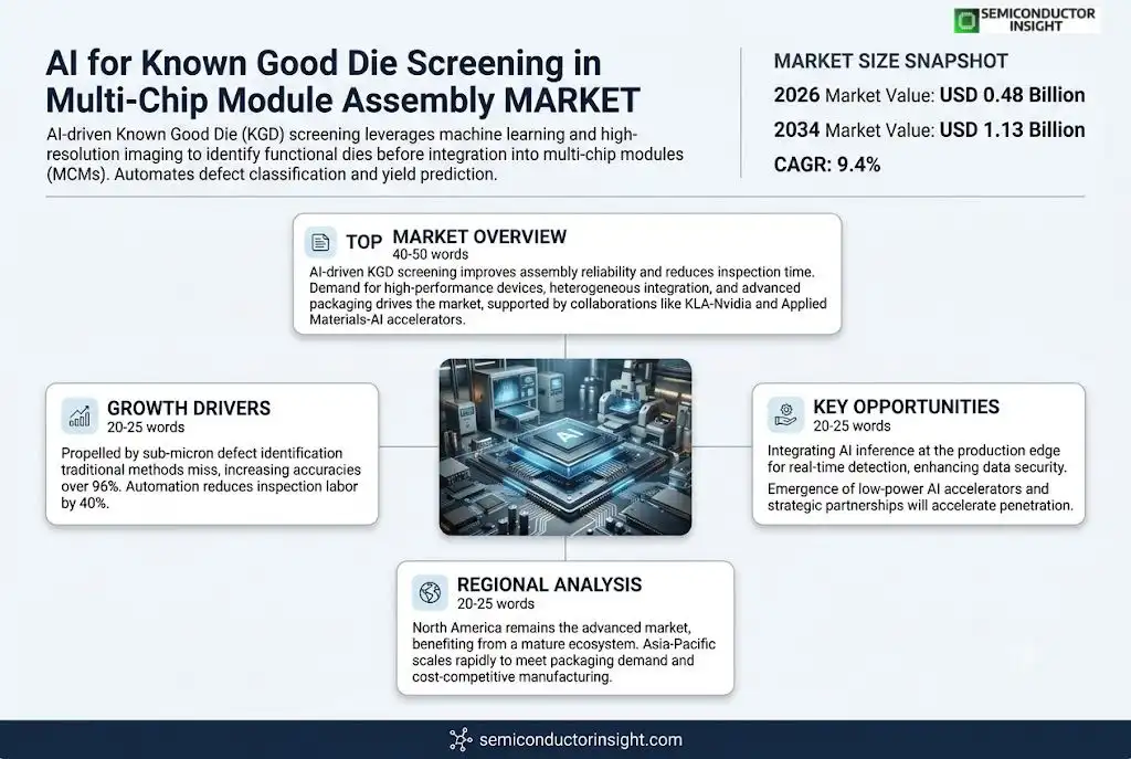
AI for Known Good Die Screening market size was valued at USD 0.46 billion in 2025. The market is projected to grow from USD 0.48 billion in 2026 to USD 1.13 billion by 2034, exhibiting a CAGR of 9.4% during the forecast period.
AI‑driven Known Good Die (KGD) screening leverages machine‑learning algorithms and high‑resolution imaging to identify functional dies before they are integrated into multi‑chip modules (MCMs). By automating defect classification and yield prediction, the technology reduces manual inspection time and improves overall assembly reliability.The market is accelerating because semiconductor manufacturers are investing heavily in advanced packaging and AI analytics to meet demand for higher performance devices. Furthermore, collaborations such as KLA’s partnership with Nvidia (2023) and Applied Materials’ integration of AI accelerators (2024) are expanding solution portfolios, while rising adoption of heterogeneous integration drives continued growth.
MARKET DRIVERS
Advanced Defect Detection Capability
The adoption of AI for Known Good Die Screening in Multi-Chip Module Assembly Market is propelled by its ability to identify sub‑micron defects that traditional optical inspection misses. Machine‑learning models trained on large image datasets can differentiate between functional and defective dies with accuracies exceeding 96%, enabling manufacturers to reduce false‑positive rates and improve yield.
Cost Efficiency and Throughput Gains
Automation of die screening reduces manual inspection labor by up to 40% and shortens cycle time per wafer. The resulting throughput increase supports the scaling of multi‑chip module (MCM) production lines, aligning with the forecasted 12% annual growth in high‑performance computing demand.
➤ “AI‑driven screening has become a decisive factor for OEMs seeking to maintain competitive margins while meeting reliability standards.”
Finally, the integration of AI platforms with existing manufacturing execution systems streamlines data flow, providing real‑time analytics that drive continuous process improvement across the MCM assembly ecosystem.
MARKET CHALLENGES
Algorithm Generalization across Diverse Die
AI models often perform optimally on the specific die families they were trained on, yet manufacturers handle a wide range of semiconductor technologies. Ensuring consistent performance across heterogeneous designs requires extensive retraining and validation, which can extend development cycles.
Other Challenges
Data Scarcity
High‑resolution testing data for emerging die architectures are limited, constraining model accuracy. Companies must invest in synthetic data generation or collaborative data‑sharing consortia to overcome this barrier.
MARKET RESTRAINTS
High Capital Expenditure
The initial outlay for AI‑powered inspection hardware, coupled with required computing infrastructure, represents a significant financial commitment. For mid‑size fabs, this cost can delay adoption despite the long‑term ROI potential.Additionally, the need for specialized integration engineers adds to the overall expense, creating a restraint for organizations with limited engineering budgets.
MARKET OPPORTUNITIES
Integration with Edge Computing
Deploying AI inference at the edge of the production line enables real‑time defect detection without reliance on centralized cloud resources. This reduces latency and enhances data security, making the solution attractive for highly regulated aerospace and defense supply chains.Furthermore, the emergence of low‑power AI accelerators expands the feasibility of on‑device screening, opening opportunities for smaller, modular fabs seeking rapid scalability.Strategic partnerships between AI software vendors and equipment manufacturers are expected to accelerate market penetration, positioning the AI for Known Good Die Screening in Multi-Chip Module Assembly Market for sustained growth over the next decade.
AI for Known Good Die Screening in Multi-Chip Module Assembly Market Trends
AI‑Enabled Yield Optimization
The introduction of AI algorithms into known good die (KGD) screening is reshaping yield management for multi‑chip module (MCM) assembly. Machine‑learning models now process high‑resolution imagery in real time, classifying defect types with accuracy that surpasses manual inspection. This capability trims inspection cycles, lowers labor exposure, and provides predictive insights that enable operators to adjust process parameters before yield losses materialize. Early adopters report a noticeable reduction in defective die insertion, which translates into higher overall module reliability and shorter time‑to‑market for advanced packaging products. The trend reflects a broader industry shift toward data‑driven quality control, where AI serves as the analytical engine for continuous improvement.
Other Trends
Collaborations Driving Technology Adoption
Strategic alliances are accelerating market momentum. In 2023, a leading inspection equipment provider teamed with a major GPU manufacturer to embed specialized inference accelerators into defect‑detection platforms. The partnership broadened the algorithmic repertoire, allowing faster adaptation to new die architectures. A subsequent 2024 integration of AI accelerators by a premier materials supplier expanded the scope of KGD screening to include thermal and electrical predictive models. These collaborations not only broaden solution portfolios but also lower entry barriers for smaller foundries seeking to incorporate AI‑based screening without extensive in‑house development.
Integration with Heterogeneous Packaging
As heterogeneous integration becomes the preferred route for high‑performance computing, the need for reliable die selection intensifies. AI‑driven KGD screening aligns with the complexity of stacking diverse die typeslogic, memory, RFby delivering granular defect analysis that respects each component’s unique failure modes. The technology enables manufacturers to curate die inventories that meet stringent thermal and electrical pairing criteria, thereby reducing rework rates during MCM assembly. This alignment between AI screening and heterogeneous packaging is expected to reinforce the competitive advantage of firms that adopt the approach, especially as product cycles shorten and market pressure for flawless integration rises.
COMPETITIVE LANDSCAPE
Key Industry Players
AI‑Driven Known Good Die Screening Competitive Landscape 2024
The market is currently dominated by a handful of semiconductor equipment leaders that have integrated AI acceleration into their Known Good Die (KGD) screening platforms. KLA Corp., leveraging its partnership with Nvidia announced in 2023, offers a high‑throughput inspection system that combines deep‑learning defect classification with predictive yield models, positioning it as the de‑facto standard for large‑volume MCM manufacturers. Applied Materials follows closely, having embedded AI accelerators into its latest KGD scanners in 2024, enabling real‑time anomaly detection and reducing cycle time by up to 30 %. Both firms benefit from extensive customer bases in advanced packaging, allowing them to shape pricing dynamics and set performance benchmarks. Secondary tier players such as ASML and Lam Research are expanding their portfolios with AI‑enhanced metrology modules, while niche specialists like Cohu Inc. and Nova Measuring Instruments focus on cost‑effective solutions for mid‑size fabs, creating a layered market structure where scale and integration depth dictate competitive positioning.Beyond the primary tier, several companies contribute significant depth to the competitive landscape. Teradyne and Advantest provide test‑centric AI platforms that complement KGD screening by validating functional performance post‑inspection. FormFactor supplies wafer‑level probing technology that feeds high‑resolution data into AI models, improving defect localization. Hitachi High‑Technologies and Samsung Electronics have launched joint AI research programs targeting heterogeneous integration, while Intel’s internal AI‑driven KGD initiatives aim to secure supply‑chain resilience for its own MCM products. Emerging startups such as DeepVision Sensors and QubitAI bring specialized machine‑learning algorithms for pattern recognition, offering boutique services to OEMs seeking differentiated yield optimization. This ecosystem of large OEMs, established equipment vendors, and agile innovators creates a competitive environment where collaboration, IP licensing, and rapid algorithmic improvement are key success factors.
List of Key AI for Known Good Die Screening Companies Profiled
- KLA Corp.
- Applied Materials Inc.
- ASML Holding
- Lam Research Corp.
- Teradyne Inc.
- Advantest Corp.
- Cohu Inc.
- Nova Measuring Instruments Ltd.
- FormFactor Inc.
- Hitachi High‑Technologies Corp.
- Samsung Electronics Co., Ltd.
- Intel Corporation
- DeepVision Sensors
- QubitAI
Segment Analysis:
| Segment Category | Sub-Segments | Key Insights |
| By Type |
|
Optical Imaging‑Based AI is emerging as the principal driver because it couples high‑resolution visual data with deep‑learning models to pinpoint subtle surface anomalies.
|
| By Application |
|
Yield Prediction delivers strategic value by forecasting the proportion of functional dies that will pass through later assembly steps.
|
| By End User |
|
Semiconductor Fab Operators are the primary adopters as AI‑enabled KGD screening directly aligns with their mandate to maximize throughput and reliability.
|
| By Integration Level |
|
Die‑to‑Die integration benefits most from AI screening because the yield of each individual die directly impacts the success of the bonded pair.
|
| By AI Technique |
|
Supervised Learning remains dominant as labeled defect datasets enable precise classification and confidence scoring.
|
Regional Analysis: AI for Known Good Die Screening in Multi-Chip Module Assembly Market
North America
AI algorithms are being embedded directly into inspection equipment, enabling real‑time defect classification and predictive maintenance. Vendors are focusing on edge‑AI solutions that minimize latency and protect proprietary process data.
Major players include large equipment manufacturers teaming with AI specialists, alongside niche firms offering bespoke model training services tailored to specific wafer technologies.
Standards agencies encourage the use of AI for quality assurance, and compliance frameworks are evolving to accommodate data‑centric validation methods without imposing heavy burdens.
Venture capital and corporate R&D budgets are increasingly allocated to AI‑driven defect detection, reflecting confidence in long‑term yield benefits and cost reductions.
Europe
European fab operators are progressing steadily, leveraging collaborative research programs funded by the EU to integrate AI into die screening workflows. The focus is on harmonizing data standards across borders, which facilitates knowledge sharing and accelerates model deployment. While adoption rates lag slightly behind North America, strong regulatory support and a growing pool of AI talent contribute to a robust pipeline of innovations.
Asia‑Pacific
Asia‑Pacific manufacturers are rapidly scaling AI solutions to meet soaring demand for high‑density packaging. Companies are investing in custom AI chips to process large image datasets locally, reducing bandwidth costs. The region’s cost‑competitive labor market and aggressive capacity expansion create a fertile environment for AI‑enhanced screening, though integration complexity remains a challenge for smaller players.
South America
In South America, early adopters are primarily large foundries that partner with AI vendors to upgrade legacy inspection systems. Market growth is driven by export-oriented production, where yield improvements directly impact competitiveness. Limited local AI expertise means most implementations rely on external consulting and training programs.
Middle East & Africa
The Middle East & Africa region is witnessing the initial stages of AI integration for die screening, driven by government initiatives to diversify economies toward advanced manufacturing. Pilot projects focus on utilizing cloud‑based AI services to offset the shortage of on‑site expertise, laying the groundwork for broader adoption as skill development programs mature.
Report Scope
This market research report provides a comprehensive analysis of the AI for Known Good Die Screening in Multi-Chip Module Assembly Market , covering the forecast period 2026–2034. It offers detailed insights into market dynamics, technological advancements, competitive landscape, and key trends shaping the industry.
Key focus areas of the report include:
- Market Overview: The report begins with an overview outlining its current market scenario, key growth indicators, and industry transformation drivers. It discusses macroeconomic factors, demand–supply balance, regulatory landscape, and the strategic role of semiconductors in powering advancements across industries such as automotive, telecommunications, consumer electronics, and industrial automation.
- Market Size & Forecast: Historical data and future projections for revenue, unit shipments, and market value across major regions and segments.
- Segmentation Analysis: Detailed breakdown by product type, technology, application, and end-user industry to identify high-growth segments and investment opportunities.
- Regional Insights: Insights into market performance across North America, Europe, Asia-Pacific, Latin America, and the Middle East & Africa, including country-level analysis where relevant.
- Competitive Landscape: Profiles of leading market participants, including their product offerings, R&D focus, manufacturing capacity, pricing strategies, and recent developments such as mergers, acquisitions, and partnerships.
- Technology Trends & Innovation: Assessment of emerging technologies, integration of AI/IoT, semiconductor design trends, fabrication techniques, and evolving industry standards.
- Market Drivers & Restraints: Evaluation of factors driving market growth along with challenges, supply chain constraints, regulatory issues, and market-entry barriers.
- Stakeholder Insights: Insights for component suppliers, OEMs, system integrators, investors, and policymakers regarding the evolving ecosystem and strategic opportunities.
Primary and secondary research methods are employed, including interviews with industry experts, data from verified sources, and real-time market intelligence to ensure the accuracy and reliability of the insights presented.
FREQUENTLY ASKED QUESTIONS:
What is the current market size of AI for Known Good Die Screening in Multi-Chip Module Assembly Market?
-> AI for Known Good Die Screening in Multi-Chip Module Assembly Market was valued at USD 0.46 billion in 2025 and is expected to reach USD 1.13 billion by 2034, indicating a CAGR of 9.4% over the forecast period.
Which key companies operate in AI for Known Good Die Screening in Multi-Chip Module Assembly Market?
-> Key players include KLA Corp., Nvidia Corporation, Applied Materials Inc., Intel Corporation, TSMC, and ASML Holding, among others.
What are the key growth drivers?
-> Key growth drivers include rising demand for advanced packaging, adoption of AI-driven defect detection, increasing heterogeneous integration, and substantial investments in semiconductor manufacturing automation.
Which region dominates the market?
-> Asia-Pacific is the fastest‑growing region, while North America remains a dominant market due to early adoption of AI analytics in semiconductor fabs.
What are the emerging trends?
-> Emerging trends include integration of AI accelerators for real‑time die screening, deployment of edge AI for on‑fab inspection, and development of mixed‑signal AI models to improve yield prediction accuracy.
Get Sample Report PDF for Exclusive Insights
Report Sample Includes
- Table of Contents
- List of Tables & Figures
- Charts, Research Methodology, and more...
 Download Sample Report PDF


