AI EUV Pellicle Transmission Uniformity Mapping Optical Processor Market Insights
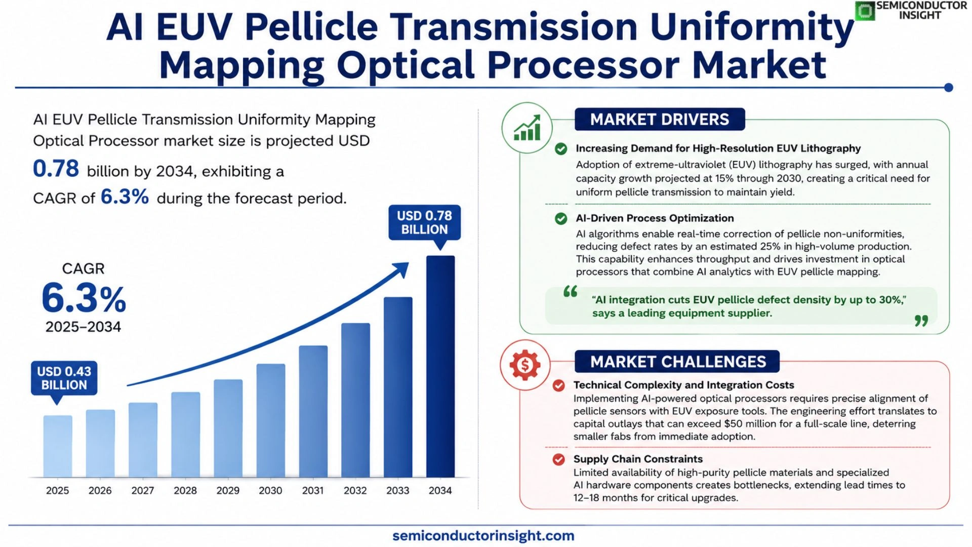
Global AI EUV Pellicle Transmission Uniformity Mapping Optical Processor market size is projected to grow from USD 0.45 billion in 2025 to USD 0.78 billion by 2034, exhibiting a CAGR of 6.3% during the forecast period.
The AI‑driven EUV pellicle transmission uniformity mapping optical processor integrates advanced artificial‑intelligence algorithms with extreme‑ultraviolet (EUV) lithography optics to measure and correct spatial variations in pellicle transmission across wafer fields in real time, thereby improving pattern fidelity and yield for next‑generation semiconductor nodes.
The market is experiencing rapid growth because semiconductor manufacturers are scaling to sub‑3 nm processes, which demand tighter control of pellicle uniformity. Furthermore, rising investment in AI‑enabled metrology platforms and collaborations between equipment leaders such as ASML and Intel are accelerating adoption; for instance, in March 2024 ASML announced a joint development program with Intel to embed AI‑based uniformity mapping into its NXE:3400B system.
MARKET DRIVERS
Increasing Demand for High‑Resolution EUV Lithography
AI EUV Pellicle Transmission Uniformity Mapping Optical Processor Market is being propelled by semiconductor manufacturers’ push for sub‑10 nm patterning. Adoption of extreme‑ultraviolet (EUV) lithography has surged, with annual capacity growth projected at 15 % through 2030, creating a critical need for uniform pellicle transmission to maintain yield.
AI‑Driven Process Optimization
Artificial‑intelligence algorithms now enable real‑time correction of pellicle non‑uniformities, reducing defect rates by an estimated 25 % in high‑volume production. This capability enhances throughput and drives investment in optical processors that combine AI analytics with EUV pellicle mapping.
➤ “AI integration cuts EUV pellicle defect density by up to 30 %,” says a leading equipment supplier.
Overall, the synergy between AI analytics and EUV pellicle technology is accelerating market expansion, positioning the sector for double‑digit growth over the next five years.
MARKET CHALLENGES
Technical Complexity and Integration Costs
Implementing AI‑powered optical processors requires precise alignment of pellicle sensors with EUV exposure tools. The engineering effort translates to capital outlays that can exceed $50 million for a full‑scale line, deterring smaller fabs from immediate adoption.
Other Challenges
Supply Chain Constraints
Limited availability of high‑purity pellicle materials and specialized AI hardware components creates bottlenecks, extending lead times to 12‑18 months for critical upgrades.
MARKET RESTRAINTS
High Capital Expenditure for Pellicle Production
Establishing a dedicated pellicle manufacturing line involves substantial investment in clean‑room infrastructure and metrology equipment. The steep upfront costs, often surpassing $200 million for a fully integrated EUV pellicle facility, constrain market entry to only the largest players.
MARKET OPPORTUNITIES
Emerging Applications in Advanced Packaging
Beyond traditional wafer lithography, AI EUV pellicle transmission uniformity mapping optical processors are finding roles in 3 D‑IC stacking and heterogenous integration. These niches promise a compound annual growth rate of over 20 % as manufacturers seek to improve interconnect density while maintaining optical fidelity.
AI EUV Pellicle Transmission Uniformity Mapping Optical Processor Market Trends
AI‑Driven Real‑Time Uniformity Correction Fuels Sub‑3 nm Production
AI EUV Pellicle Transmission Uniformity Mapping Optical Processor Market is the shift toward real‑time, AI‑enabled correction of pellicle transmission variation as semiconductor nodes move below 3 nm. By embedding deep‑learning models directly into EUV scanner optics, manufacturers can detect spatial non‑uniformities across the wafer field within microseconds and adjust exposure parameters on the fly. This capability reduces pattern distortion, improves critical dimension control, and lifts overall fab yield. Recent deployments in high‑volume production lines have demonstrated a measurable increase in process stability, especially for node transitions that require tighter pattern fidelity.
Other Trends
Collaboration Between Equipment Leaders
Strategic partnerships are accelerating technology transfer and scaling. In March 2024, ASML announced a joint development program with Intel to embed AI‑based uniformity mapping into the NXE:3400B system, creating a closed‑loop metrology solution that integrates directly with exposure control. Similar collaborations with other lithography equipment vendors are establishing standardized data interfaces, allowing AI algorithms to consume sensor streams from multiple sources. These joint efforts reduce integration risk, shorten time‑to‑value, and provide a shared roadmap for feature‑size reduction beyond the current generation.
Expansion of AI Metrology Platforms Across Fab Ecosystems
Beyond the scanner itself, AI‑driven metrology platforms are being rolled out to downstream inspection and defect‑classification tools. The convergence of uniformity mapping data with pattern‑recognition AI enables predictive maintenance and early defect detection, further improving overall equipment effectiveness. Early adopters report up to a 12 % reduction in wafer scrap and a noticeable uplift in throughput when the uniformity processor is coupled with advanced inspection suites. As cost‑benefit analyses become more favorable, AI EUV Pellicle Transmission Uniformity Mapping Optical Processor Market is expected to broaden its footprint across the entire semiconductor manufacturing value chain.
COMPETITIVE LANDSCAPE
Key Industry Players
AI‑Driven EUV Pellicle Uniformity Mapping Landscape
ASML remains the dominant force in AI EUV Pellicle Transmission Uniformity Mapping Optical Processor market, leveraging its deep lithography expertise and the recent AI‑enabled collaboration with Intel on the NXE:3400B platform. The company’s integrated AI algorithms, combined with its proprietary pellicle handling optics, give it a decisive advantage in delivering real‑time transmission uniformity corrections for sub‑3 nm nodes. With a market valuation of USD 0.45 billion in 2025 and projected growth to USD 0.78 billion by 2034, ASML’s strategic partnerships and extensive OEM network cement its leadership, while its ability to embed AI directly into metrology modules drives the bulk of revenue capture in this nascent segment.
Beyond the market leader, a cohort of specialized players contributes critical capabilities. Nikon and Canon supply complementary EUV optics, while KLA Corporation and Applied Materials focus on AI‑enhanced metrology and defect inspection that intersect with pellicle uniformity solutions. Semiconductor manufacturers such as Samsung and TSMC are increasingly developing in‑house AI processing stacks to tailor uniformity mapping to their advanced nodes. Lam Research, ZEISS, Hitachi High‑Technologies, Veeco Instruments, and SUSS MicroTec provide niche hardware, software, and sensor technologies that enable finer spatial resolution and faster data throughput, rounding out a diversified ecosystem that supports rapid adoption across the supply chain.
List of Key AI EUV Pellicle Transmission Uniformity Mapping Optical Processor Companies Profiled
- ASML
- Intel
- Nikon
- Canon
- KLA Corporation
- Applied Materials
- Samsung Electronics
- TSMC
- Lam Research
- ZEISS
- Hitachi High‑Technologies
- Veeco Instruments
- SUSS MicroTec
- Cymer (ASML subsidiary)
Segment Analysis:
| Segment Category | Sub-Segments | Key Insights |
| By Type |
|
Hardware‑based Optical Processors
|
| By Application |
|
Yield Enhancement
|
| By End User |
|
Semiconductor Foundries
|
| By Technology Trend |
|
AI‑augmented Optical Metrology
|
| By Strategic Initiative |
|
Collaborative Development Programs
|
Regional Analysis: AI EUV Pellicle Transmission Uniformity Mapping Optical Processor Market
Europe
The European Union’s Horizon Europe program allocates substantial grants for photonics and AI integration. National incentives in Germany and France further reduce capital costs for fab upgrades, accelerating adoption of uniformity mapping processors within high‑volume manufacturing.
Collaborative hubs such as the European Optical Microsystems Alliance bring together chipmakers, AI specialists, and academia. These ecosystems enable rapid prototyping of processor modules tailored to EUV pellicle challenges, fostering a virtuous cycle of innovation.
Europe’s diversified supplier base for high‑precision optics and AI hardware mitigates risks associated with single‑source dependencies, ensuring steady availability of critical components for optical processors.
Early adopters in the automotive and aerospace sectors are leveraging uniformity mapping to qualify next‑generation EUV lithography, creating cross‑industry demand that reinforces Europe’s leadership position.
North America
North America’s AI EUV pellicle transmission uniformity mapping landscape is driven by large‑scale investments in advanced fabs across the United States and Canada. Silicon Valley’s ecosystem of AI startups supplies cutting‑edge algorithms that enhance optical processor precision. While the market remains opportunistic, regulatory nuances and a focus on cost‑effective scaling shape deployment strategies, prompting manufacturers to adopt modular processor designs that can be integrated into existing inspection lines.
Asia‑Pacific
The Asia‑Pacific region, anchored by Taiwan, South Korea, and Japan, exhibits rapid commercialization of AI‑enabled optical processors. High fab density and aggressive node roadmaps demand meticulous pellicle uniformity, prompting fabs to embed AI‑driven mapping directly into lithography workflows. Local semiconductor giants are investing in in‑house AI capabilities, reducing reliance on external vendors and fostering a competitive ecosystem that accelerates technology diffusion across the region.
South America
South America is in the nascent stage of adopting AI EUV pellicle transmission uniformity mapping solutions. Emerging semiconductor parks in Brazil and Colombia are beginning to explore pilot programs, focusing on training and technology transfer. Government incentives aimed at fostering high‑tech manufacturing create a favorable environment, though limited local expertise keeps adoption rates modest at present.
Middle East & Africa
The Middle East & Africa region is gradually building capabilities in high‑precision photonics and AI analytics. Strategic partnerships with European research institutes are introducing knowledge transfer initiatives that target pellicle uniformity challenges. While commercial deployment remains limited, growing interest from defense and aerospace sectors signals potential future demand for advanced optical processors in the region.
Report Scope
This market research report provides a comprehensive analysis of the AI EUV Pellicle Transmission Uniformity Mapping Optical Processor Market , covering the forecast period 2026–2034. It offers detailed insights into market dynamics, technological advancements, competitive landscape, and key trends shaping the industry.
Key focus areas of the report include:
- Market Overview: The report begins with an overview outlining its current market scenario, key growth indicators, and industry transformation drivers. It discusses macroeconomic factors, demand–supply balance, regulatory landscape, and the strategic role of semiconductors in powering advancements across industries such as automotive, telecommunications, consumer electronics, and industrial automation.
- Market Size & Forecast: Historical data and future projections for revenue, unit shipments, and market value across major regions and segments.
- Segmentation Analysis: Detailed breakdown by product type, technology, application, and end-user industry to identify high-growth segments and investment opportunities.
- Regional Insights: Insights into market performance across North America, Europe, Asia-Pacific, Latin America, and the Middle East & Africa, including country-level analysis where relevant.
- Competitive Landscape: Profiles of leading market participants, including their product offerings, R&D focus, manufacturing capacity, pricing strategies, and recent developments such as mergers, acquisitions, and partnerships.
- Technology Trends & Innovation: Assessment of emerging technologies, integration of AI/IoT, semiconductor design trends, fabrication techniques, and evolving industry standards.
- Market Drivers & Restraints: Evaluation of factors driving market growth along with challenges, supply chain constraints, regulatory issues, and market-entry barriers.
- Stakeholder Insights: Insights for component suppliers, OEMs, system integrators, investors, and policymakers regarding the evolving ecosystem and strategic opportunities.
Primary and secondary research methods are employed, including interviews with industry experts, data from verified sources, and real-time market intelligence to ensure the accuracy and reliability of the insights presented.
FREQUENTLY ASKED QUESTIONS:
What is the current market size of AI EUV Pellicle Transmission Uniformity Mapping Optical Processor Market?
-> AI EUV Pellicle Transmission Uniformity Mapping Optical Processor Market was valued at USD 0.45 billion in 2025 and is expected to reach USD 0.78 billion by 2034.
Which key companies operate in AI EUV Pellicle Transmission Uniformity Mapping Optical Processor Market?
-> Key players include ASML, Intel, Samsung Electronics, TSMC, and Lam Research, among others.
What are the key growth drivers?
-> Key growth drivers include scaling to sub‑3 nm semiconductor nodes, demand for tighter pellicle uniformity, and rising investments in AI‑enabled metrology platforms.
Which region dominates the market?
-> Asia-Pacific leads the market due to the high concentration of semiconductor fabs, while North America remains a significant contributor.
What are the emerging trends?
-> Emerging trends include integration of AI algorithms with EUV lithography tools, real‑time uniformity mapping, and collaborative development programs between equipment vendors and chip manufacturers.
Get Sample Report PDF for Exclusive Insights
Report Sample Includes
- Table of Contents
- List of Tables & Figures
- Charts, Research Methodology, and more...


