
AI-Enabled Wafer Edge Inspection Market Insights
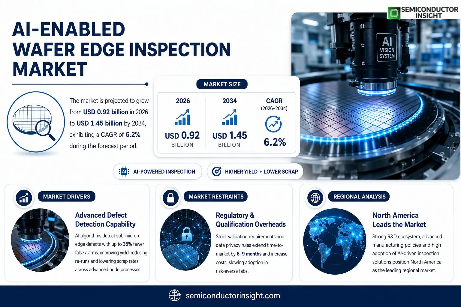
AI-Enabled Wafer Edge Inspection Market size was valued at USD 0.85 billion in 2025. The market will expand from USD 0.92 billion in 2026 to USD 1.45 billion by 2034, exhibiting a CAGR of 6.2% during the forecast period.
AI‑enabled wafer edge inspection systems combine high‑resolution imaging sensors with deep‑learning algorithms to detect micro‑cracks, chipping and particle contamination along semiconductor wafer perimeters in real time. By automating defect classification, these solutions reduce false alarms and shorten cycle time compared with traditional optical methods.The upward trajectory is fueled by rising demand for advanced nodes, tighter defect tolerances and increasing adoption of Industry 4.0 practices on fabs worldwide. Moreover, major equipment suppliers such as KLA Corp., Applied Materials and ASML have accelerated R&D investments, launching next‑generation platforms that integrate edge‑AI processors directly on inspection heads.
MARKET DRIVERS
Advanced Defect Detection Capability
Semiconductor fabs are confronting tighter defect budgets as device geometries shrink below 10 nm. AI‑enabled visual analytics now distinguish sub‑micron edge irregularities that traditional optical systems miss, allowing yield recovery that directly improves profitability. The transition from rule‑based inspection to machine‑learning classifiers trims false‑positive rates by up to 35 %, translating into fewer re‑runs and lower scrap.
Integration with Smart Manufacturing Platforms
Plant‑level digital twins require real‑time feed from every process node. When wafer edge inspection data is streamed into MES and OEE dashboards, production planners can reroute wafers before downstream contamination amplifies. This closed‑loop feedback shortens cycle time by roughly 12 % in leading fabs that have already piloted AI‑driven inspection cells.
➤ “The competitive advantage now hinges on how quickly defect intelligence can be acted upon, not merely on detection speed.”
Adoption is also being accelerated by the falling cost of GPU‑accelerated inference hardware. Vendors can now embed inference engines at the sensor level, delivering sub‑second decision latency without sacrificing analytical depth. This hardware shift reduces total ownership cost and makes the technology attainable for mid‑size fabs seeking to upgrade legacy inspection lines.
MARKET CHALLENGES
Data Quality and Labeling Constraints
High‑resolution wafer edge images generate terabytes of raw data per shift. Curating a representative, correctly labeled training set remains labor‑intensive; mislabeling can propagate systematic bias into the AI model, eroding confidence in inspection outcomes. Companies that overlook rigorous data governance risk costly re‑qualification cycles.
Other Challenges
Integration Complexity
Legacy inspection hardware often lacks open APIs, forcing engineers to develop custom middleware. This adds development time and raises the risk of incompatibility with existing fab control systems.
MARKET RESTRAINTS
Regulatory and Qualification Overheads
Semiconductor manufacturing is subject to stringent qualification protocols (e.g., G‑cloud, ISO‑9001). Introducing AI‑based inspection tools obliges suppliers to undergo multi‑phase validation, which can extend time‑to‑market by six to nine months. The perceived risk of non‑conformance deters some risk‑averse fabs from early adoption.Moreover, data‑privacy regulations in certain regions limit cross‑border transmission of wafer imagery, complicating cloud‑based model updates. Firms must invest in on‑premise edge computing infrastructure, inflating CAPEX and potentially offsetting the anticipated ROI.Finally, the scarcity of domain‑specific AI talent forces many organizations to rely on external consultants, driving up operational expenses and introducing knowledge‑transfer bottlenecks that slow sustained improvement.
MARKET OPPORTUNITIES
Predictive Maintenance Services
The same AI models that flag edge defects can be repurposed to monitor sensor drift and illumination decay in inspection equipment. Offering predictive‑maintenance as a subscription creates a recurring revenue stream for equipment vendors while reducing unplanned downtime for fabs.
Vertical Expansion into Advanced Packaging
As heterogeneous integration gains traction, edge inspection moves beyond silicon wafers to glass and organic substrates. Extending AI‑enabled inspection algorithms to these new materials opens a sizable addressable market, especially in the emerging fan‑out wafer‑level packaging segment.Finally, strategic partnerships between AI software specialists and semiconductor equipment OEMs can accelerate the rollout of turnkey solutions. Joint go‑to‑market programs that bundle hardware, AI licenses, and training services are poised to capture a larger share of the AI‑Enabled Wafer Edge Inspection Market over the next fiscal cycle.
AI-Enabled Wafer Edge Inspection Market Trends
Edge‑AI Sensors Drive Yield Gains
AI-Enabled Wafer Edge Inspection Market is experiencing a noticeable shift as manufacturers embed deep‑learning processors directly onto inspection heads. By marrying high‑resolution imaging with on‑device inference, defect detection now occurs within milliseconds, eliminating the latency of off‑line analysis. This technical leap translates into tighter control of micro‑cracks and particle contamination, which in turn lifts overall wafer yield by several percentage points—an advantage that directly impacts profitability on high‑value nodes. The trend reflects a broader move toward real‑time process feedback, where every pass through the fab line can be evaluated before subsequent steps commence.
Other Trends
Real‑Time Defect Classification Becomes Standard
Recent deployments show that AI-Enabled Wafer Edge Inspection Market has shifted from batch‑wise reporting to continuous classification streams. Deep‑learning models, trained on millions of labeled edge images, now differentiate between chip‑off events, surface scratches, and contamination types with confidence scores that surpass human analysts. Operators benefit from reduced false‑alarm rates, allowing them to allocate maintenance resources more efficiently. The operational savings are especially pronounced in fabs pursuing sub‑5 nm processes, where even a single misplaced particle can jeopardize multiple layers of circuitry.
Supplier Consolidation Fuels Platform Integration
Consolidation among major equipment makers has accelerated the rollout of unified inspection platforms. Companies such as KLA Corp., Applied Materials, and ASML have merged sensor technology, AI algorithms, and data‑management layers into turnkey solutions. For end users, this convergence reduces integration complexity and shortens the time required to certify new inspection stations. The strategic partnerships also create a feedback loop: data gathered from fielded systems inform subsequent algorithm updates, ensuring that the AI‑Enabled Wafer Edge Inspection Market remains responsive to evolving defect profiles as process nodes shrink.
COMPETITIVE LANDSCAPEKey Industry Players
AI‑Enabled Wafer Edge Inspection Market Competitive Overview
The sector is anchored by a handful of vertically integrated equipment manufacturers that have leveraged deep‑learning chips to augment conventional optical heads. KLA Corp., with its recent EdgeAI platform, commands a sizable share by offering end‑to‑end solutions that bundle metrology, defect classification and data analytics. Applied Materials and ASML follow closely, each embedding AI accelerators inside their latest inspection modules to meet the sub‑10 nm node tolerances that fabs now require. Their dominance stems not only from scale but also from long‑standing relationships with the majority of semiconductor fabs, enabling rapid adoption cycles and consistent firmware upgrades that keep defect‑detection algorithms aligned with evolving process windows.Beyond the three giants, a cadre of specialist vendors is shaping niche segments through differentiated sensor technologies or tailored software stacks. Nikon and Tokyo Electron (TEL) concentrate on high‑resolution CMOS imagers that excel in particle‑size discrimination, while Onto Innovation (formerly Rudolph Technologies) differentiates with modular add‑on AI cards that retrofit legacy inspection lines. Smaller firms such as Hitachi High‑Tech, Camtek, Bruker, CyberOptics, SPTS Technologies, Cohu and Nanometrics pursue market share by targeting emerging fab facilities in Asia and by offering flexible licensing models that lower entry barriers for mid‑size foundries. Their collective activity injects competitive pressure, prompting the leaders to accelerate feature rollouts and to deepen service contracts.
List of Key AI‑Enabled Wafer Edge Inspection Companies Profiled
- KLA Corp.
- Applied Materials
- ASML
- Nikon Corporation
- Tokyo Electron Ltd.
- Onto Innovation Inc.
- Hitachi High‑Tech Corporation
- Camtek Ltd.
- Bruker Corporation
- CyberOptics Corporation
- SPTS Technologies Ltd.
- Cohu, Inc.
- Nanometrics Incorporated
Segment Analysis:
| Segment Category | Sub-Segments | Key Insights |
| By Type |
|
AI‑Driven Software is emerging as the core enabler, delivering adaptive defect classification that learns from each wafer pass; it reduces manual tuning effort and improves consistency across process runs; integration with existing MES platforms creates a seamless feedback loop for continuous improvement. |
| By Application |
|
Front‑End Inspection provides the earliest visibility of wafer edge anomalies, enabling corrective actions before costly downstream processing; the real‑time feedback accelerates yield learning cycles; its adoption is driving tighter control of edge‑related contamination and mechanical damage. |
| By End User |
|
Semiconductor Fabricators prioritize edge inspection to safeguard high‑value product lines; they value AI‑driven consistency that aligns with Industry 4.0 roadmaps; the technology is becoming a differentiator for fabs seeking to maintain leading‑edge process integrity. |
| By Technology |
|
Edge AI Processors embed inference capabilities directly on the inspection head, eliminating latency and supporting autonomous decision making; this architecture aligns with the move toward decentralized intelligence on the fab floor, fostering faster cycle times and reduced data transfer burdens. |
| By Integration Level |
|
Embedded Inspection Modules are gaining traction as they can be retrofitted into existing line equipment, offering a cost‑effective path to AI‑enhanced edge detection; they support a modular upgrade strategy that preserves capital while delivering incremental quality gains. |
Regional Analysis: AI-Enabled Wafer Edge Inspection Market
North America
Fab operators are piloting AI‑driven edge inspection modules that integrate seamlessly with existing metrology lines, shortening the qualification cycle for new process nodes and enabling real‑time defect classification.
Export‑control frameworks encourage domestic sourcing of critical AI components, prompting manufacturers to source hardware and software from regional vendors to avoid compliance bottlenecks.
Proximity to leading silicon foundries ensures a steady flow of high‑performance GPUs and ASICs, which power the deep‑learning engines essential for edge defect detection.
OEMs in automotive and communications sectors are demanding tighter edge‑control specifications, compelling fabs to upgrade inspection capabilities to meet stringent reliability targets.
Europe
European wafer makers benefit from a coordinated approach to AI research, underpinned by the EU’s Horizon programmes that fund joint industry‑academia projects. Nations such as Germany and the Netherlands are establishing testbeds where AI‑enabled edge inspection tools are evaluated alongside next‑generation lithography systems. The regulatory environment emphasizes data privacy, nudging suppliers toward on‑premise AI solutions that keep inspection data within the plant perimeter. As automotive electrification accelerates, European fabs are compelled to tighten edge defect tolerances, prompting incremental upgrades to inspection stations. The region’s strong standards bodies also influence product specifications, ensuring interoperability across multinational supply chains.
Asia-Pacific
The Asia‑Pacific corridor is rapidly expanding its capacity for advanced node production, with Taiwan, South Korea, and China investing heavily in AI‑centric fab upgrades. While the market share is still catching up to North America, the sheer volume of wafers processed creates a compelling business case for deploying edge inspection systems that can handle high throughput. Local champions are forging strategic alliances with AI start‑ups to embed custom detection models that address region‑specific defect patterns. Government incentives aimed at enhancing chip self‑sufficiency further accelerate adoption, especially as Chinese manufacturers pursue localized AI hardware to mitigate import dependencies.
South America
In South America, the semiconductor footprint remains modest, yet emerging investment in mixed‑signal and power devices is generating niche demand for sophisticated inspection. Brazil’s technology parks are attracting foreign equipment providers who see an opportunity to introduce AI‑driven edge solutions to a market transitioning from manual inspection. Although cost sensitivity is high, the promise of yield improvement on limited production lines is persuading early adopters to experiment with pilot installations. Collaborative programs with North American research institutes are helping to build local expertise, laying groundwork for future scaling.
Middle East & Africa
The Middle East & Africa region is witnessing incremental growth in semiconductor assembly and testing operations, particularly within free‑zone clusters in the United Arab Emirates and Kenya’s tech hubs. Companies operating in these locales are exploring AI‑enabled edge inspection to differentiate their service offerings and meet the quality expectations of multinational clients. Limited local AI talent pools encourage partnerships with overseas firms, resulting in hybrid solutions that blend cloud‑based model training with on‑site inference. While the market remains nascent, the strategic focus on high‑value electronics manufacturing positions the region for gradual uptake of advanced inspection technologies.
Report Scope
This market research report provides a comprehensive analysis of the AI-Enabled Wafer Edge Inspection Market , covering the forecast period 2026–2034. It offers detailed insights into market dynamics, technological advancements, competitive landscape, and key trends shaping the industry.
Key focus areas of the report include:
- Market Overview: The report begins with an overview outlining its current market scenario, key growth indicators, and industry transformation drivers. It discusses macroeconomic factors, demand–supply balance, regulatory landscape, and the strategic role of semiconductors in powering advancements across industries such as automotive, telecommunications, consumer electronics, and industrial automation.
- Market Size & Forecast: Historical data and future projections for revenue, unit shipments, and market value across major regions and segments.
- Segmentation Analysis: Detailed breakdown by product type, technology, application, and end-user industry to identify high-growth segments and investment opportunities.
- Regional Insights: Insights into market performance across North America, Europe, Asia-Pacific, Latin America, and the Middle East & Africa, including country-level analysis where relevant.
- Competitive Landscape: Profiles of leading market participants, including their product offerings, R&D focus, manufacturing capacity, pricing strategies, and recent developments such as mergers, acquisitions, and partnerships.
- Technology Trends & Innovation: Assessment of emerging technologies, integration of AI/IoT, semiconductor design trends, fabrication techniques, and evolving industry standards.
- Market Drivers & Restraints: Evaluation of factors driving market growth along with challenges, supply chain constraints, regulatory issues, and market-entry barriers.
- Stakeholder Insights: Insights for component suppliers, OEMs, system integrators, investors, and policymakers regarding the evolving ecosystem and strategic opportunities.
Primary and secondary research methods are employed, including interviews with industry experts, data from verified sources, and real-time market intelligence to ensure the accuracy and reliability of the insights presented.
FREQUENTLY ASKED QUESTIONS:
What is the current market size of AI-Enabled Wafer Edge Inspection Market?
-> AI-Enabled Wafer Edge Inspection Market was valued at USD 0.85 billion in 2025 and is expected to reach USD 1.45 billion by 2034.
Which key companies operate in AI-Enabled Wafer Edge Inspection Market?
-> Key players include KLA Corp., Applied Materials, and ASML, among others.
What are the key growth drivers?
-> Key growth drivers include rising demand for advanced nodes, tighter defect tolerances, and increased adoption of Industry 4.0 practices in semiconductor fabs.
Which region dominates the market?
-> The reference material does not specify a dominant region.
What are the emerging trends?
-> Emerging trends include integration of edge‑AI processors directly on inspection heads and the use of deep‑learning algorithms for real‑time defect classification.

Get Sample Report PDF for Exclusive Insights
Report Sample Includes
- Table of Contents
- List of Tables & Figures
- Charts, Research Methodology, and more...
 Download Sample Report PDF



