
AI-Enabled High-NA EUV Lithography Process Control Market Insights
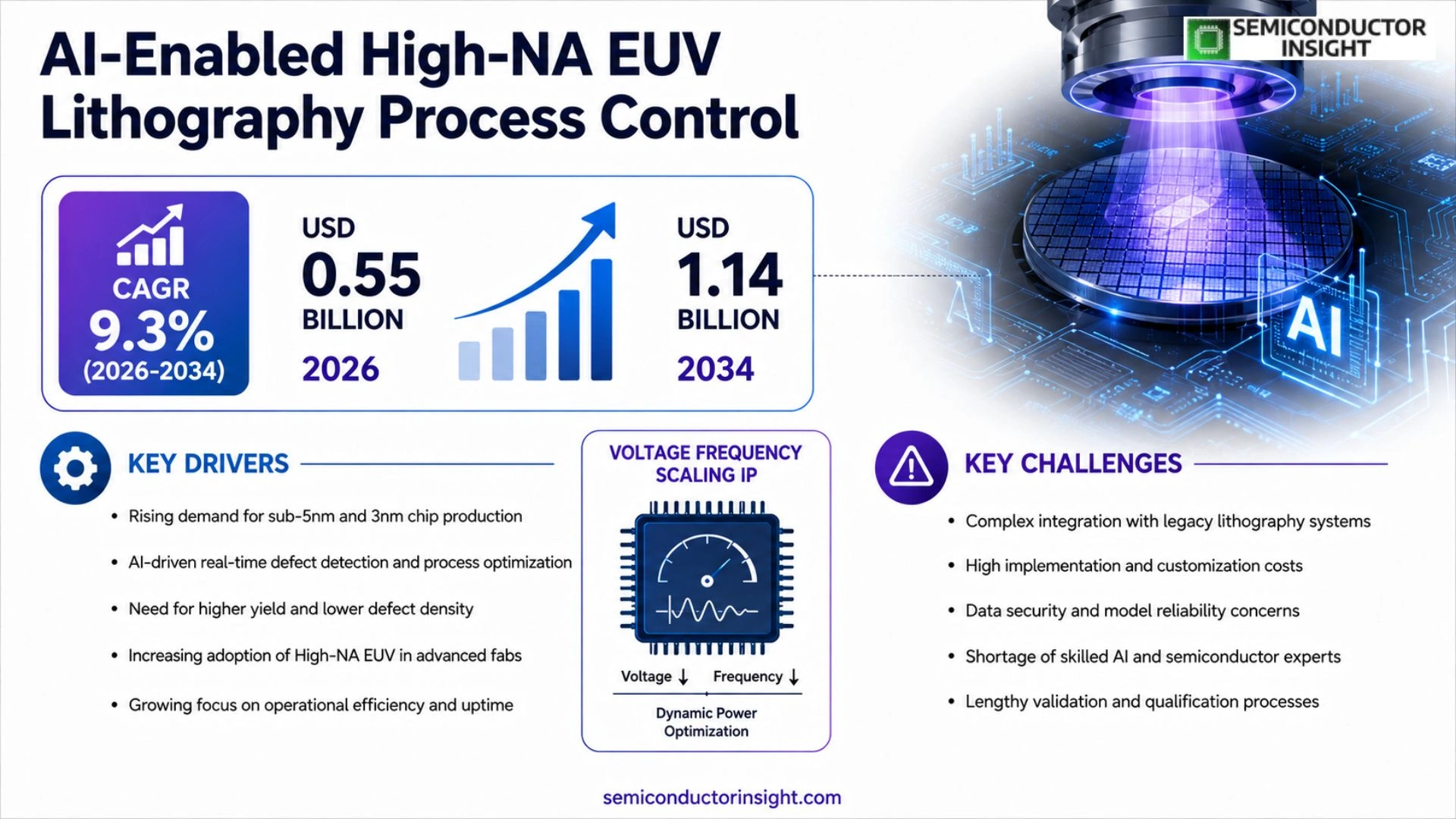
Global AI-enabled High-NA EUV Lithography Process Control market size was valued at USD 0.48 billion in 2025. The market is forecasted to expand from USD 0.55 billion in 2026 to USD 1.14 billion by 2034, reflecting a CAGR of 9.3% over the forecast horizon.
AI‑enabled High‑NA EUV lithography process control merges sophisticated machine‑learning models with extreme‑ultraviolet scanners that possess numerical apertures greater than 0.55 µm. By continuously ingesting exposure data, predicting mask defects, and fine‑tuning focus and dose on the fly, the technology lifts wafer yield and shortens cycle time for leading‐edge nodes such as 3 nm and beyond.
The upward trajectory stems from mounting capital outlays on high‑NA EUV equipment, surging demand for sub‑5 nm chips, and an industry shift toward data‑centric fab operations. Recent collaborations,most notably the ASML partnership announced in March 2024 with an AI analytics firm,accelerate uptake because they lower the expertise threshold for deterministic process control. At the same time, semiconductor manufacturers are earmarking larger shares of R&D spend for AI‑driven metrology and defect detection, reinforcing the market’s momentum.
MARKET DRIVERS
Increasing Chip Complexity Fuels Demand for Precision Control
As semiconductor nodes progress below 5 nm, manufacturers confront tighter tolerances for pattern fidelity. AI‑enabled analytics deliver sub‑nanometer insight into photon‑to‑photoresist interactions, allowing fabs to extract higher yield from each wafer. This technical pressure directly lifts interest in the AI‑Enabled High‑NA EUV Lithography Process Control Market, where operators seek to close the gap between design intent and printed reality.
Cost‑Pressure Incentivizes Predictive Maintenance
High‑NA EUV tools represent capital outlays exceeding $150 million per unit. Unplanned downtime erodes profitability quickly, prompting fabs to adopt predictive‑maintenance models powered by machine‑learning. By correlating sensor streams with defect patterns, AI reduces mean‑time‑to‑repair and justifies the premium of the AI‑Enabled High‑NA EUV Lithography Process Control Market.
➤ “Data‑driven process control is now the decisive factor between leading‑edge yield and marginal performance.”
Regulatory pushes toward lower power consumption also reshape tool operation. Advanced AI systems can recalibrate exposure parameters in real time, trimming energy use without sacrificing throughput. Consequently, chipmakers view sophisticated process‑control platforms as essential, creating a sustained upward pressure on market adoption.
MARKET CHALLENGES
Integration Complexity Hinders Rapid Roll‑Out
Embedding AI modules within legacy EUV suites demands extensive software‑hardware alignment. Existing control stacks were not engineered for high‑velocity data ingestion, leading to prolonged validation cycles. This friction slows the transition of the AI‑Enabled High‑NA EUV Lithography Process Control Market from pilot to full‑scale deployment.
Other Challenges
Talent Scarcity
The niche combination of photonics expertise and deep‑learning proficiency remains rare. Companies compete fiercely for a handful of specialists capable of tuning neural‑network models to lithographic physics, inflating recruitment costs and extending project timelines.
MARKET RESTRAINTS
High Initial Capital Expenditure
The acquisition of a high‑NA EUV scanner already pushes budget ceilings; adding AI‑enabled control layers introduces additional software licences, sensors, and integration services. For many mid‑size fabs, the total cost of ownership remains a prohibitive barrier, tempering broader market penetration.
Data Security Concerns
Process data contains proprietary design rules and yield‑critical parameters. Firms wary of exposing such information to cloud‑based AI platforms may opt for on‑premise solutions, which are often more expensive and slower to implement, thereby restraining market growth.
Regulatory Uncertainty
Emerging standards around AI auditability in semiconductor manufacturing are still evolving. Unclear compliance pathways can deter investment, as fabs prefer to defer AI augmentation until clear guidelines are established.
MARKET OPPORTUNITIES
Hybrid Cloud‑Edge Architectures for Real‑Time Control
Deploying inference engines at the equipment edge while leveraging cloud resources for model training offers a compelling value proposition. This architecture reduces latency in critical loop‑control decisions and simultaneously scales analytical power, positioning the AI‑Enabled High‑NA EUV Lithography Process Control Market to capture a new segment of performance‑oriented fabs.
Collaborative Standardization Initiatives
Industry consortia are drafting open APIs for lithography data exchange. Early adopters that align their AI solutions with these standards can benefit from interoperability, faster integration, and reduced customization costs,creating a first‑mover advantage.
Expansion into Advanced Packaging
Beyond logic chips, high‑NA EUV is entering advanced packaging workflows where alignment tolerances are equally stringent. AI‑driven process control can translate directly to this adjacent market, unlocking additional revenue streams for vendors and expanding the addressable universe of the AI‑Enabled High‑NA EUV Lithography Process Control Market.
AI-Enabled High-NA EUV Lithography Process Control Market Trends
Capital Investment and Yield Enhancement
The transition to High‑NA EUV scanners is reshaping fab economics. As manufacturers allocate larger portions of capex to equipment that exceeds 0.55 µm numerical aperture, the need for real‑time process control intensifies. AI‑enabled algorithms now ingest exposure data every few milliseconds, allowing the system to anticipate focus drift and dose deviations before they manifest as yield loss. This predictive capability translates into a measurable uptick in wafer throughput for nodes at 3 nm and finer, where each percentage point of yield carries a hefty revenue impact.
Other Trends
AI‑Driven Defect Detection
Modern defect‑inspection stations pair high‑resolution imaging with convolutional networks trained on millions of defect signatures. The result is a reduction in false‑positive rates, which frees engineering resources for higher‑value troubleshooting. Because the models update continuously from live production data, they adapt to pattern shifts introduced by new mask designs, keeping the detection cycle tightly aligned with design‑for‑manufacture constraints.
Collaborative Ecosystem Development
Strategic alliances are accelerating market adoption. The March 2024 partnership between ASML and a leading AI analytics firm exemplifies how hardware vendors are bundling software intelligence to lower the skill barrier for deterministic control. Such collaborations not only expedite deployment but also create joint‑IP that can be leveraged across multiple fabs, reducing the overhead of custom model development. Meanwhile, semiconductor manufacturers are earmarking a growing slice of R&D budgets for AI‑centric metrology, signaling a shift toward data‑first fab strategies that will reshape vendor‑customer dynamics.
COMPETITIVE LANDSCAPE
Key Industry Players
AI‑Enabled High‑NA EUV Lithography Process Control – Competitive Landscape
The market revolves around a handful of firms that control both the hardware platform and the algorithmic layer. ASML remains the linchpin, supplying the majority of high‑NA EUV scanners while simultaneously embedding proprietary machine‑learning modules that adjust focus, dose, and mask‑defect prediction in real time. Its recent collaboration with an AI‑analytics specialist, announced in early 2024, exemplifies a strategy of bundling sophisticated software with the scanner’s optical core, thereby reducing the skill barrier for fab engineers and accelerating adoption at leading‑edge fabs. This dual‑track approach has generated a de‑facto standard, pressuring downstream adopters to align with ASML’s roadmap and creating a high entry threshold for new entrants.
Beyond the dominant supplier, a constellation of chipmakers and equipment vendors is shaping the ecosystem. Intel, Samsung Electronics, and TSMC have each rolled out internal AI‑control stacks that interface with ASML hardware, leveraging deep‑learning models trained on proprietary process data to squeeze additional yield out of sub‑5 nm nodes. Applied Materials and KLA Corp supply metrology and inspection tools that feed high‑frequency data into these models, while Lam Research’s deposition solutions complement the control loop by adjusting material thickness in response to AI‑driven recommendations. Software specialists such as Synopsys and Cadence provide the simulation environments that validate algorithmic updates before fab deployment. Niche players,including CVC, GlobalFoundries, and NXP Semiconductors,focus on vertical integration of AI for specific device families, positioning themselves as agile alternatives for midsize fabs seeking customized solutions.
List of Key AI‑Enabled High‑NA EUV Lithography Process Control Companies Profiled
- ASML Holding
- Intel Corporation
- Samsung Electronics
- TSMC
- Applied Materials
- KLA Corp
- Lam Research
- Synopsys
- Cadence Design Systems
- CVC
- GlobalFoundries
- NXP Semiconductors
- Canon
- Nikon
- Thermo Fisher Scientific
Segment Analysis:
| Segment Category | Sub-Segments | Key Insights |
| By Type |
|
Hardware‑centric solutions
|
| By Application |
|
Focus and dose optimization
|
| By End User |
|
Leading‑edge fab operators
|
| By Technology |
|
Hybrid AI‑physics approaches
|
| By Process Stage |
|
Exposure control
|
Regional Analysis: AI-Enabled High-NA EUV Lithography Process Control Market
AI-driven recipe optimization is now embedded in pilot lines, allowing operators to predict focus drift before it manifests. Early adopters report noticeable yield improvements, prompting broader rollout across high‑volume fabs.
Recent tax credits for advanced manufacturing equipment have lowered the effective cost of AI‑enhanced EUV tools, encouraging capital re‑allocation toward smarter process‑control environments.
Vertical integration between sensor manufacturers and AI software firms is reducing data latency, enabling near‑real‑time adjustments that were previously impossible in the lithography workflow.
Universities are launching joint photonics‑AI programs, producing graduates who can bridge process engineering and machine‑learning, a scarce skill set that fuels market momentum.
Europe
European fabs are leveraging the continent’s strong standards‑setting bodies to embed AI verification modules into EUV tool firmware. While investment cycles are slightly longer than in North America, the region’s emphasis on sustainable manufacturing drives the development of energy‑aware AI models that minimize power draw during high‑volume production. Collaborative projects funded by the European Horizon program are creating open datasets that lower entry barriers for smaller equipment vendors, gradually democratizing the technology across both mature and leading‑edge nodes.
Asia-Pacific
In the Asia-Pacific, the market is propelled by massive capacity expansions in East Asian foundries, where throughput pressure forces rapid AI integration. Local chipmakers are co‑developing proprietary neural‑network architectures tuned to the peculiarities of their process chemistries, achieving finer control over stochastic defects. Government‑backed “smart factory” initiatives provide a regulatory cushion that accelerates pilot deployments, while the region’s dense supplier network ensures quick hardware iterations to match AI software upgrades.
South America
South American semiconductor activities remain nascent, yet the region is positioning itself as a testbed for low‑cost AI‑enabled lithography pilots. Partnerships between multinational equipment manufacturers and regional research institutes focus on adapting high‑NA EUV control algorithms to modest fab environments, emphasizing cost‑effective yield improvement rather than absolute performance. This pragmatic approach could cultivate a niche market for scalable AI solutions that later mature into broader offerings.
Middle East & Africa
Middle East & Africa exhibit limited direct involvement in High‑NA EUV production, but they are cultivating a supportive ecosystem through heavy investment in data‑centers and AI research hubs. By attracting AI talent and fostering cross‑border collaborations, these economies aim to become downstream analytics providers for global lithography players, offering specialized services such as defect classification and process‑parameter recommendation engines.
Report Scope
This market research report provides a comprehensive analysis of the AI-Enabled High-NA EUV Lithography Process Control Market , covering the forecast period 2026–2034. It offers detailed insights into market dynamics, technological advancements, competitive landscape, and key trends shaping the industry.
Key focus areas of the report include:
- Market Overview: The report begins with an overview outlining its current market scenario, key growth indicators, and industry transformation drivers. It discusses macroeconomic factors, demand–supply balance, regulatory landscape, and the strategic role of semiconductors in powering advancements across industries such as automotive, telecommunications, consumer electronics, and industrial automation.
- Market Size & Forecast: Historical data and future projections for revenue, unit shipments, and market value across major regions and segments.
- Segmentation Analysis: Detailed breakdown by product type, technology, application, and end-user industry to identify high-growth segments and investment opportunities.
- Regional Insights: Insights into market performance across North America, Europe, Asia-Pacific, Latin America, and the Middle East & Africa, including country-level analysis where relevant.
- Competitive Landscape: Profiles of leading market participants, including their product offerings, R&D focus, manufacturing capacity, pricing strategies, and recent developments such as mergers, acquisitions, and partnerships.
- Technology Trends & Innovation: Assessment of emerging technologies, integration of AI/IoT, semiconductor design trends, fabrication techniques, and evolving industry standards.
- Market Drivers & Restraints: Evaluation of factors driving market growth along with challenges, supply chain constraints, regulatory issues, and market-entry barriers.
- Stakeholder Insights: Insights for component suppliers, OEMs, system integrators, investors, and policymakers regarding the evolving ecosystem and strategic opportunities.
Primary and secondary research methods are employed, including interviews with industry experts, data from verified sources, and real-time market intelligence to ensure the accuracy and reliability of the insights presented.
FREQUENTLY ASKED QUESTIONS:
What is the current market size of AI-Enabled High-NA EUV Lithography Process Control Market?
-> AI-Enabled High-NA EUV Lithography Process Control Market was valued at USD 0.48 billion in 2025 and is expected to reach USD 1.14 billion by 2034.
Which key companies operate in AI-Enabled High-NA EUV Lithography Process Control Market?
-> Key players include Axalta Coating Systems, AkzoNobel, BASF SE, PPG, Sherwin-Williams, and 3M, among others.
What are the key growth drivers?
-> Key growth drivers include railway infrastructure investments, urbanization, and demand for durable coatings.
Which region dominates the market?
-> Asia-Pacific is the fastest-growing region, while Europe remains a dominant market.
What are the emerging trends?
-> Emerging trends include bio-based coatings, smart coatings, and sustainable rail solutions.

Get Sample Report PDF for Exclusive Insights
Report Sample Includes
- Table of Contents
- List of Tables & Figures
- Charts, Research Methodology, and more...
 Download Sample Report PDF




