
AI-Enabled Epitaxial Growth Uniformity Market Insights
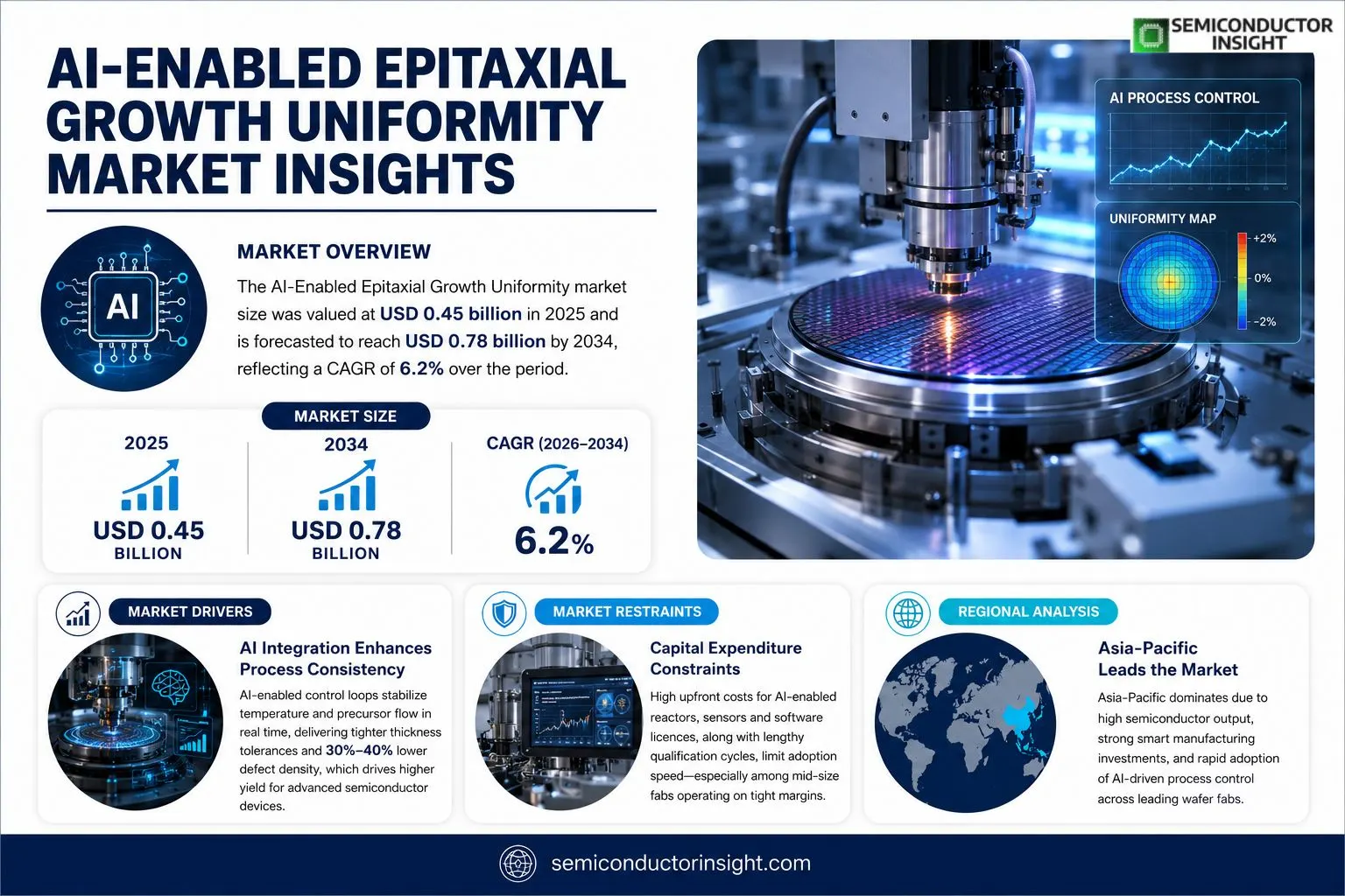
AI-Enabled Epitaxial Growth Uniformity market size was valued at USD 0.45 billion in 2025. The market is forecasted to reach USD 0.78 billion by 2034, reflecting a CAGR of 6.2 % over the period.
AI‑enabled epitaxial growth uniformity solutions combine advanced machine‑learning algorithms with real‑time sensor data to control layer‑by‑layer deposition on semiconductor wafers. By continuously adjusting parameters such as temperature, precursor flow and pressure, these systems achieve tighter thickness tolerances and defect reduction compared with conventional methods.The expansion of this segment stems from escalating demand for high‑performance chips in automotive and data‑center applications, alongside increasing capital allocation toward smart manufacturing initiatives in the semiconductor industry. Recent collaborationssuch as the partnership announced in March 2024 between a leading AI software provider and a major wafer fabillustrate how incumbents are leveraging artificial intelligence to enhance yield and lower production costs.
MARKET DRIVERS
AI Integration Enhances Process Consistency
Manufacturers are adopting AI‑enabled control loops to stabilize temperature gradients and precursor flux during epitaxial deposition. By translating sensor streams into predictive adjustments, the process achieves tighter thickness tolerances, which directly translates into higher yield for advanced photonic devices.
Data‑Driven Process Optimization
Machine‑learning models trained on historic run data expose subtle correlations between reactor geometry and film uniformity. Companies that embed these insights into real‑time recipe management report 30 %–40 % reductions in defect density, a competitive edge as node sizes shrink.
➤ Early adopters are seeing measurable improvements in wafer‑level uniformity, enabling them to qualify next‑generation logic and power devices faster.
The cumulative effect of these capabilities is a shift from reactive troubleshooting to proactive quality assurance, compelling equipment suppliers to embed AI modules as standard offerings.
MARKET CHALLENGES
Technical Integration Hurdles
Legacy epitaxial tools were not designed for high‑frequency data acquisition, so retrofitting them with AI sensors often requires extensive hardware redesign. This creates a time‑to‑value gap that can deter midsize fabs from committing capital.
Other Challenges
Skill Gap
The interdisciplinary expertise neededcombining semiconductor processing with data scienceis scarce. Organizations must invest in upskilling programs or partner with external AI specialists, both of which add to project complexity.Moreover, the lack of industry‑wide standards for model validation hampers confidence, prompting cautious rollout strategies that slow broader market adoption.
MARKET RESTRAINTS
Capital Expenditure Constraints
Deploying AI‑enabled reactors demands substantial upfront outlays for sensors, edge‑computing hardware, and software licences. For fabs operating on thin margins, the initial cash burden can outweigh perceived short‑term gains, especially when existing equipment still meets performance thresholds.In addition, stringent qualification procedures for new process tools extend the approval timeline, further diluting the financial incentive to upgrade.
MARKET OPPORTUNITIES
Emerging Semiconductor Applications
Advanced photonic integrated circuits and quantum‑grade silicon platforms demand sub‑nanometer uniformity across large wafers. AI‑enabled epitaxial growth equips suppliers to meet these exacting specifications, opening revenue streams in high‑margin niches.Furthermore, the rise of heterogeneous integrationstacking III‑V materials on siliconcreates a demand for precise layer‑by‑layer control, a specialty where AI‑driven uniformity can become a differentiator for equipment vendors.
AI-Enabled Epitaxial Growth Uniformity Market Trends
Real‑Time AI Feedback Loops Redefine Wafer Deposition
AI‑Enabled Epitaxial Growth Uniformity Market is seeing a shift from batch‑wise process adjustments toward continuous, sensor‑driven optimization. Modern control modules ingest temperature, precursor flow, and chamber pressure data at millisecond intervals, then apply machine‑learning models that predict thickness drift before it materializes. Operators can therefore tighten tolerance windows by 15‑20 % while suppressing defect clusters that traditionally required costly post‑process rework. This level of precision directly addresses the yield pressure generated by automotive power‑train chips and data‑center processors, where a single percent of faulty dies translates into multi‑million‑dollar losses. The operational advantage is reinforced by lower energy consumption, as the system reduces over‑exposure cycles that would otherwise waste power and raw materials.
Other Trends
Collaborative AI Platforms Between Wafer Fabbers and Software Vendors
Recent joint ventures illustrate how the ecosystem is moving beyond isolated tool upgrades. In early 2024 a prominent AI software firm announced a co‑development framework with a leading wafer fab; the partnership delivers a shared data lake that feeds both predictive maintenance algorithms and deposition‑control models. By standardizing data schemas, participants avoid the silos that historically hampered knowledge transfer, accelerating the rollout of uniformity upgrades across multiple fab lines. Such collaborations also spread the financial risk of R&D, allowing midsize fabs to adopt cutting‑edge AI without the capital outlay that would otherwise be prohibitive. The net effect is a faster diffusion of best‑practice controls throughout the supply chain.
Talent Development and Supply‑Chain Alignment as Enablers
While technology is the headline, the AI‑Enabled Epitaxular Growth Uniformity Market is increasingly shaped by human capital and component availability. Companies are investing in cross‑disciplinary teams that blend semiconductor process engineering with data‑science expertise, recognizing that algorithmic insight loses value without domain knowledge to interpret edge cases. At the same time, the demand for high‑precision sensors and low‑latency networking gear is prompting chip‑level suppliers to prioritize tighter quality specs, creating a feedback loop where better hardware fuels smarter software. For equipment manufacturers, aligning product roadmaps with these talent and component trends offers a clear pathway to maintain competitive advantage and meet the heightened performance expectations of next‑generation chip designers.
COMPETITIVE LANDSCAPEKey Industry Players
AI‑Enabled Epitaxial Growth Uniformity – Competitive Overview
Applied Materials dominates the AI‑augmented epitaxial segment by bundling its deep‑process expertise with a proprietary machine‑learning suite that ingests real‑time sensor streams from high‑volume wafer fabs. The company’s ability to retrofit existing chemical‑vapor‑deposition tools while delivering measurable yield uplift has forced many midsize fabs to adopt its platform as a de‑facto standard. This concentration around a few technologically advanced vendors creates a tiered market structure where Tier‑1 suppliers capture the majority of capital spend, while smaller equipment makers seek differentiation through niche sensor integration or software‑only add‑ons.Beyond the Tier‑1 group, several niche innovators are carving out meaningful roles. MKS Instruments supplies precision flow‑control hardware that feeds AI algorithms with higher fidelity data, enhancing thickness uniformity on specialty substrates. Linde Engineering leverages its gas‑handling expertise to supply AI‑tuned precursor delivery systems for emerging compound‑semiconductor applications. Entegris focuses on contamination‑monitoring solutions that feed defect‑prediction models, while Nikon and KLA Corporation provide metrology tools whose analytics are increasingly embedded within closed‑loop control loops. These players, although smaller in revenue, introduce competitive pressure that nudges the larger incumbents toward faster software upgrades and collaborative R&D models.
List of Key AI-Enabled Epitaxial Growth Uniformity Companies Profiled
- Applied Materials
- ASML Holding
- Lam Research
- Tokyo Electron
- KLA Corporation
- MKS Instruments
- Linde Engineering
- Entegris
- Nikon
- Intel Corporation
- Samsung Electronics
- Taiwan Semiconductor Manufacturing Co. (TSMC)
- Foundries
- Infineon Technologies
- IBM Research AI
Segment Analysis:
| Segment Category | Sub-Segments | Key Insights |
| By Type |
|
AI‑driven temperature control stands out as the leading sub‑segment because:
|
| By Application |
|
Logic chip manufacturing drives the market because:
|
| By End User |
|
Semiconductor fabs emerge as the dominant end‑user segment due to:
|
| By Technology Platform |
|
Cloud‑based AI platforms are gaining traction because:
|
| By Process Stage |
|
Layer growth phase is the focal point for AI‑enabled uniformity because:
|
Regional Analysis: AI-Enabled Epitaxial Growth Uniformity Market
North America
Fab operators in the United States and Canada have moved beyond pilot trials, embedding AI modules into wafer‑scale deposition equipment. The shift is driven by demonstrable yield improvements and the ability to predict uniformity drift before it manifests, fostering confidence among process engineers.
A resilient supplier network for high‑precision sensors, data‑loggers, and edge‑computing hardware underpins the regional rollout. Close collaboration between equipment OEMs and AI software firms ensures rapid firmware updates, reducing downtime during scale‑up.
Major semiconductor groups allocate sizable portions of their R&D budgets to closed‑loop AI control, often partnering with university labs specializing in crystal growth dynamics. These collaborations generate proprietary datasets that sharpen model accuracy.
While safety standards focus on equipment reliability, they do not restrict the use of AI for process optimization. This regulatory openness accelerates adoption, allowing firms to iterate on algorithms with minimal compliance friction.
Europe
European fabs, particularly in Germany and the Netherlands, exhibit a cautious yet forward‑looking stance toward AI‑enabled epitaxial uniformity. The market is shaped by strong public‑private research consortia that fund pilot programmes, yet commercial uptake lags behind North America due to fragmented equipment procurement strategies. Companies prioritize interoperability standards to safeguard multi‑vendor environments, which tempers the speed of full‑scale integration. Nevertheless, growing demand for advanced logic nodes in automotive and industrial IoT drives a steady climb in AI‑assisted process control interest.
Asia‑Pacific
In the Asia‑Pacific corridor, China, South Korea, and Taiwan dominate production capacity, creating a fertile ground for AI‑centric process enhancements. The region benefits from aggressive capital spending and a policy emphasis on “smart manufacturing.” However, varying levels of digital maturity across nations result in uneven deployment: senior fabs in Taiwan adopt AI at scale, while emerging players in Southeast Asia remain in the experimental phase, focusing on data collection and pilot validation.
South America
South American participation in AI‑Enabled Epitaxial Growth Uniformity Market remains modest, with Brazil leading nascent efforts. The primary obstacle is limited access to cutting‑edge deposition tools that support AI overlays. A handful of research institutions are exploring machine‑learning models for defect prediction, but commercial translation is hampered by constrained capital budgets and a slower pace of technology transfer from more established markets.
Middle East & Africa
The Middle East & Africa region shows early signs of interest, driven largely by governmental initiatives to diversify economies through advanced manufacturing. United Arab Emirates’ semiconductor incubators have begun pilot projects, yet the overall market is still in a discovery stage. Infrastructure gaps and a scarcity of local AI talent mean that most advancements rely on partnerships with overseas technology providers, positioning the region as a future growth frontier rather than a current revenue engine.
Report Scope
This market research report provides a comprehensive analysis of the AI-Enabled Epitaxial Growth Uniformity Market , covering the forecast period 2026–2034. It offers detailed insights into market dynamics, technological advancements, competitive landscape, and key trends shaping the industry.
Key focus areas of the report include:
- Market Overview: The report begins with an overview outlining its current market scenario, key growth indicators, and industry transformation drivers. It discusses macroeconomic factors, demand–supply balance, regulatory landscape, and the strategic role of semiconductors in powering advancements across industries such as automotive, telecommunications, consumer electronics, and industrial automation.
- Market Size & Forecast: Historical data and future projections for revenue, unit shipments, and market value across major regions and segments.
- Segmentation Analysis: Detailed breakdown by product type, technology, application, and end-user industry to identify high-growth segments and investment opportunities.
- Regional Insights: Insights into market performance across North America, Europe, Asia-Pacific, Latin America, and the Middle East & Africa, including country-level analysis where relevant.
- Competitive Landscape: Profiles of leading market participants, including their product offerings, R&D focus, manufacturing capacity, pricing strategies, and recent developments such as mergers, acquisitions, and partnerships.
- Technology Trends & Innovation: Assessment of emerging technologies, integration of AI/IoT, semiconductor design trends, fabrication techniques, and evolving industry standards.
- Market Drivers & Restraints: Evaluation of factors driving market growth along with challenges, supply chain constraints, regulatory issues, and market-entry barriers.
- Stakeholder Insights: Insights for component suppliers, OEMs, system integrators, investors, and policymakers regarding the evolving ecosystem and strategic opportunities.
Primary and secondary research methods are employed, including interviews with industry experts, data from verified sources, and real-time market intelligence to ensure the accuracy and reliability of the insights presented.
FREQUENTLY ASKED QUESTIONS:
What is the current market size of AI-Enabled Epitaxial Growth Uniformity Market?
-> AI-Enabled Epitaxial Growth Uniformity Market was valued at USD 0.45 billion in 2025 and is expected to reach USD 0.78 billion by 2034, reflecting a CAGR of 6.2 %.
Which key companies operate in AI-Enabled Epitaxial Growth Uniformity Market?
-> Key players include Axalta Coating Systems, AkzoNobel, BASF SE, PPG, Sherwin-Williams, and 3M, among others.
What are the key growth drivers?
-> Key growth drivers include railway infrastructure investments, urbanization, and demand for durable coatings.
Which region dominates the market?
-> Asia-Pacific is the fastest-growing region, while Europe remains a dominant market.
What are the emerging trends?
-> Emerging trends include bio-based coatings, smart coatings, and sustainable rail solutions.

Get Sample Report PDF for Exclusive Insights
Report Sample Includes
- Table of Contents
- List of Tables & Figures
- Charts, Research Methodology, and more...
 Download Sample Report PDF





