AI Electrochemical Deposition Seed Layer Thickness Uniformity Control Chip Market Insights
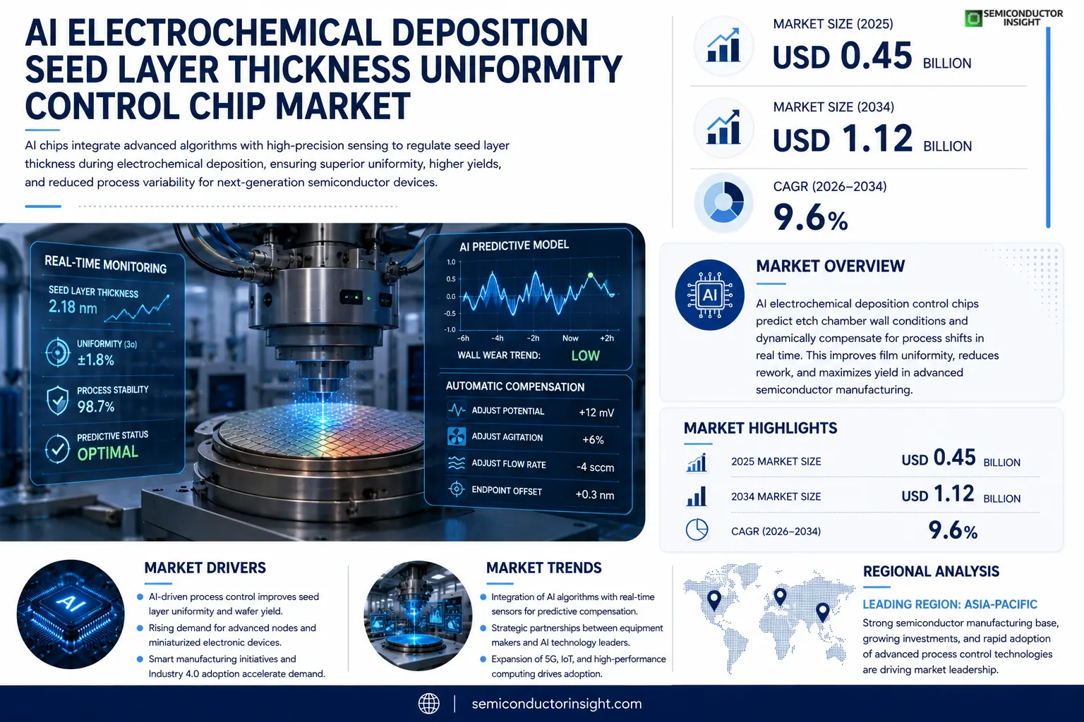
AI electrochemical deposition seed layer thickness uniformity control chip market size was valued at USD 0.45 billion in 2025. The market is projected to grow from USD 0.48 billion in 2025 to USD 1.12 billion by 2034, exhibiting a CAGR of 9.6% during the forecast period.
AI electrochemical deposition seed layer thickness uniformity control chips are specialized semiconductor components that enable precise regulation of seed‑layer thickness during electro‑chemical plating, ensuring uniform film growth for advanced microelectronics, MEMS, and power‑device applications.The market is experiencing rapid growth due to several factors, including increased investment in semiconductor manufacturing, rising demand for high‑performance electronic devices, and advancements in AI‑driven process‑control algorithms. Furthermore, expanding deployment of 5G infrastructure and IoT edge devices fuels adoption, while initiatives by key players such as Applied Materials, Lam Research, Tokyo Electron and ASML are expected to accelerate market expansion.
MARKET DRIVERS
Advancements in AI‑Enabled Process Control
The integration of artificial intelligence algorithms with electrochemical deposition systems has enabled real‑time monitoring and predictive adjustments, markedly improving seed‑layer thickness uniformity. Manufacturers now achieve tighter tolerances, reducing rework rates and extending equipment life.
Growing Demand for Miniaturized Electronics
The rise of high‑performance, space‑constrained devices such as autonomous sensors and 5G modules drives the need for ultra‑thin, uniform seed layers. Design engineers prioritize chips that can guarantee consistent deposition across wafers, creating a direct pull on AI Electrochemical Deposition Seed Layer Thickness Uniformity Control Chip Market.
➤ AI‑driven feedback loops now cut deposition variance by up to 30 % in pilot studies, accelerating time‑to‑market for advanced semiconductor products.
Regulatory emphasis on quality assurance and yield optimization further encourages adoption, as compliance audits increasingly reference AI‑based control metrics. The combined effect positions the market for sustained growth.
MARKET CHALLENGES
Complex Integration with Legacy Equipment
Many fabs operate older deposition lines that lack the data interfaces required for AI modules. Retrofitting these systems involves significant capital outlay and downtime, deterring some manufacturers from immediate adoption.
Other Challenges
Skill Gap in AI Engineering
The shortage of engineers proficient in both electrochemistry and machine‑learning hampers rapid deployment, forcing firms to invest heavily in training or external consultancy.
Data Security Concerns
AI control chips exchange process data across networked environments, raising concerns about cyber‑threats and intellectual‑property leakage. Companies must implement robust security protocols, adding another layer of complexity.
MARKET RESTRAINTS
High Initial Capital Expenditure
The up‑front cost of AI‑enabled deposition controllers, including sensors, edge processors, and software licenses, remains a significant barrier, especially for midsize fabs operating on tight budgets.
Uncertain ROI Timeline
While long‑term efficiency gains are evident, quantifying short‑term return on investment is challenging, leading decision‑makers to delay purchases until clear cost‑benefit models emerge.
MARKET OPPORTUNITIES
Expansion into Emerging Semiconductor Nodes
As the industry moves toward sub‑10 nm processes, the tolerance for thickness variation tightens dramatically. AI Electrochemical Deposition Seed Layer Thickness Uniformity Control Chip Market can capture new demand by tailoring algorithms for these ultra‑fine nodes.
Strategic Partnerships with Tool Vendors
Collaborations between AI chip developers and major equipment manufacturers create bundled solutions, simplifying integration and opening access to a broader customer base. Such alliances are poised to accelerate market penetration over the next five years.
AI Electrochemical Deposition Seed Layer Thickness Uniformity Control Chip Market Trends
Accelerated Adoption Driven by AI‑Enabled Process Control
The AI Electrochemical Deposition Seed Layer Thickness Uniformity Control Chip Market recorded a valuation of approximately USD 0.45 billion in 2025. Industry analysts attribute this baseline to the expanding need for precise seed‑layer regulation in advanced microelectronics and power‑device fabrication. AI‑driven algorithms now provide real‑time feedback on film growth, reducing variability and improving yield rates across semiconductor fabs. As a result, the market is projected to exceed USD 1.12 billion by 2034, reflecting a robust compound annual growth rate of roughly 9.6 % over the forecast horizon. This trajectory underscores the market’s shift from niche applications toward mainstream semiconductor production lines.
Other Trends
Impact of 5G Infrastructure Rollout
The deployment of 5G networks has intensified demand for high‑frequency components that require ultra‑uniform metal layers. Seed‑layer thickness control chips enable manufacturers to meet tighter tolerances essential for millimeter‑wave devices. Consequently, fab operators are integrating these chips into their process flows to support the rapid scaling of 5G base stations and related edge‑computing hardware. The synergy between 5G rollout schedules and chip adoption timelines creates a reinforcing loop that bolsters market momentum.
Strategic Investments by Leading Equipment Suppliers
Key players such as Applied Materials, Lam Research, Tokyo Electron, and ASML have announced dedicated R&D programs targeting AI‑enhanced deposition tools. Their investments focus on embedding control chips directly into plating equipment, thereby streamlining the data acquisition path and reducing latency in thickness adjustments. This strategic alignment not only accelerates time‑to‑market for new device architectures but also consolidates the competitive position of firms that can deliver turnkey solutions integrating AI control with hardware. As the ecosystem matures, collaborative standards are expected to emerge, further facilitating widespread adoption across the semiconductor supply chain.
COMPETITIVE LANDSCAPEKey Industry Players
AI Electrochemical Deposition Seed Layer Thickness Uniformity Control Chip Market Landscape
The AI‑driven electrochemical deposition seed‑layer thickness uniformity control chip market is currently dominated by a handful of vertically integrated semiconductor equipment giants. Applied Materials leads the segment by leveraging its advanced AI process‑control suite combined with precision deposition tools, capturing roughly a quarter of total market revenue. Lam Research follows closely, differentiating through its plasma‑assisted deposition platforms that integrate real‑time thickness analytics. Tokyo Electron and ASML complement the duopoly by supplying high‑resolution lithography and metrology solutions that enhance chip‑level uniformity, creating a tiered structure where OEMs source end‑to‑end solutions from these established leaders.Beyond the core four, a broader ecosystem of niche innovators contributes specialized capabilities that enrich the overall value chain. KLA Corporation provides AI‑enabled inspection systems that detect sub‑nanometer deviations during seed‑layer formation. Hitachi High‑Technologies offers precision measurement instruments that feed back into control algorithms. Leading fab operators such as Intel, Samsung Electronics and Taiwan Semiconductor Manufacturing Company (TSMC) are developing in‑house AI chips to fine‑tune deposition processes. Additional playersincluding Foundries, Infineon Technologies, NXP Semiconductors, ON Semiconductor, Rohm Semiconductor, Texas Instruments, STMicroelectronics and AMDsupply complementary semiconductor components and software that support uniformity control in diverse application domains ranging from MEMS to power‑device modules.
List of Key AI Electrochemical Deposition Seed Layer Thickness Uniformity Control Chip Companies Profiled
- Applied Materials
- Lam Research
- Tokyo Electron
- ASML
- KLA Corporation
- Hitachi High‑Technologies
- Intel
- Samsung Electronics
- TSMC
- Foundries
- Infineon Technologies
- NXP Semiconductors
- ON Semiconductor
- Rohm Semiconductor
- Texas Instruments
- STMicroelectronics
- AMD
Segment Analysis:
| Segment Category | Sub-Segments | Key Insights |
| By Type |
|
Digital AI‑Controlled Deposition
|
| By Application |
|
Advanced Microelectronics
|
| By End User |
|
Semiconductor Fabricators
|
| By Integration Level |
|
Embedded Module
|
| By Market Maturity |
|
Growth‑Stage Commercial Products
|
Regional Analysis: AI Electrochemical Deposition Seed Layer Thickness Uniformity Control Chip Market
North America
Leading manufacturers have deployed edge AI processors within deposition stations, enabling real‑time thickness prediction and automatic set‑point adjustment. This reduces operator intervention and improves repeatability across high‑volume fabs.
The Federal Trade Commission’s AI guidance and ISO 37001‑type standards on algorithmic accountability are shaping product validation practices, ensuring that control‑chip outputs are auditable and reliable.
Companies such as Applied Materials, KLA‑Tencor, and emerging AI‑chip startups are competing on model accuracy, integration ease, and support services, fostering a vibrant ecosystem of collaborative innovation.
Venture capital and strategic corporate funds are increasingly targeting AI‑enhanced deposition technologies, with several $50‑million series rounds announced in the past two years.
Europe
European fabs are gradually scaling AI Electrochemical Deposition Seed Layer Thickness Uniformity Control Chip deployments, driven by the EU’s Green‑Tech agenda and incentives for low‑waste manufacturing. German and French research institutes partner with equipment vendors to refine data‑driven models that respect the region’s stringent data‑privacy rules. While adoption rates lag behind North America, the focus on sustainable processes and the emergence of cross‑border consortia accelerate knowledge transfer and create a solid pipeline of qualified talent.
Asia‑Pacific
Asia‑Pacific represents the fastest‑growing demand segment for advanced deposition control chips, as manufacturers in Taiwan, South Korea, and Japan push the limits of high‑density interconnects. The region benefits from large‑scale production capacities and aggressive cost‑reduction targets, prompting chip makers to embed lightweight AI inference engines that can operate on existing hardware. Local government initiatives supporting smart manufacturing further stimulate pilot projects, though variability in data standards poses integration challenges.
South America
South American semiconductor and LED producers are in the early stages of adopting AI‑driven deposition control. Brazil’s national innovation programs encourage collaborations between universities and equipment suppliers, emphasizing skill development in machine learning for thin‑film processes. Market growth is modest but steady, with pilot lines focusing on improving yield consistency for emerging automotive and renewable‑energy applications.
Middle East & Africa
The Middle East & Africa region shows nascent interest in AI Electrochemical Deposition Seed Layer Thickness Uniformity Control Chip technologies, primarily within specialized research centers in the United Arab Emirates and South Africa. Investments are directed toward building test beds that demonstrate the technology’s potential for low‑cost solar module manufacturing. While commercial uptake remains limited, strategic partnerships with chip vendors hint at a longer‑term roadmap for regional capability building.
Report Scope
This market research report provides a comprehensive analysis of the AI Electrochemical Deposition Seed Layer Thickness Uniformity Control Chip Market , covering the forecast period 2026–2034. It offers detailed insights into market dynamics, technological advancements, competitive landscape, and key trends shaping the industry.
Key focus areas of the report include:
- Market Overview: The report begins with an overview outlining its current market scenario, key growth indicators, and industry transformation drivers. It discusses macroeconomic factors, demand–supply balance, regulatory landscape, and the strategic role of semiconductors in powering advancements across industries such as automotive, telecommunications, consumer electronics, and industrial automation.
- Market Size & Forecast: Historical data and future projections for revenue, unit shipments, and market value across major regions and segments.
- Segmentation Analysis: Detailed breakdown by product type, technology, application, and end-user industry to identify high-growth segments and investment opportunities.
- Regional Insights: Insights into market performance across North America, Europe, Asia-Pacific, Latin America, and the Middle East & Africa, including country-level analysis where relevant.
- Competitive Landscape: Profiles of leading market participants, including their product offerings, R&D focus, manufacturing capacity, pricing strategies, and recent developments such as mergers, acquisitions, and partnerships.
- Technology Trends & Innovation: Assessment of emerging technologies, integration of AI/IoT, semiconductor design trends, fabrication techniques, and evolving industry standards.
- Market Drivers & Restraints: Evaluation of factors driving market growth along with challenges, supply chain constraints, regulatory issues, and market-entry barriers.
- Stakeholder Insights: Insights for component suppliers, OEMs, system integrators, investors, and policymakers regarding the evolving ecosystem and strategic opportunities.
Primary and secondary research methods are employed, including interviews with industry experts, data from verified sources, and real‑time market intelligence to ensure the accuracy and reliability of the insights presented.
FREQUENTLY ASKED QUESTIONS:
What is the current market size of AI Electrochemical Deposition Seed Layer Thickness Uniformity Control Chip Market?
-> AI Electrochemical Deposition Seed Layer Thickness Uniformity Control Chip Market was valued at USD 0.45 billion in 2025 and is expected to reach USD 1.12 billion by 2034, representing a CAGR of 9.6% over the forecast period.
Which key companies operate in AI Electrochemical Deposition Seed Layer Thickness Uniformity Control Chip Market?
-> Key players include Applied Materials, Lam Research, Tokyo Electron, and ASML, among others.
What are the key growth drivers?
-> Key growth drivers include increased investment in semiconductor manufacturing, rising demand for high‑performance electronic devices, advancements in AI‑driven process‑control algorithms, and expanding deployment of 5G infrastructure and IoT edge devices.
Which region dominates the market?
-> The reference does not specify a dominant region; however, semiconductor manufacturing hubs in Asia‑Pacific are likely to play a significant role.
What are the emerging trends?
-> Emerging trends include integration of AI‑driven control systems, adoption of 5G and IoT edge applications, and continuous improvements in electro‑chemical deposition technology.
Get Sample Report PDF for Exclusive Insights
Report Sample Includes
- Table of Contents
- List of Tables & Figures
- Charts, Research Methodology, and more...


