
AI-Driven Nanosheet Transistor Process Optimization Market Insights
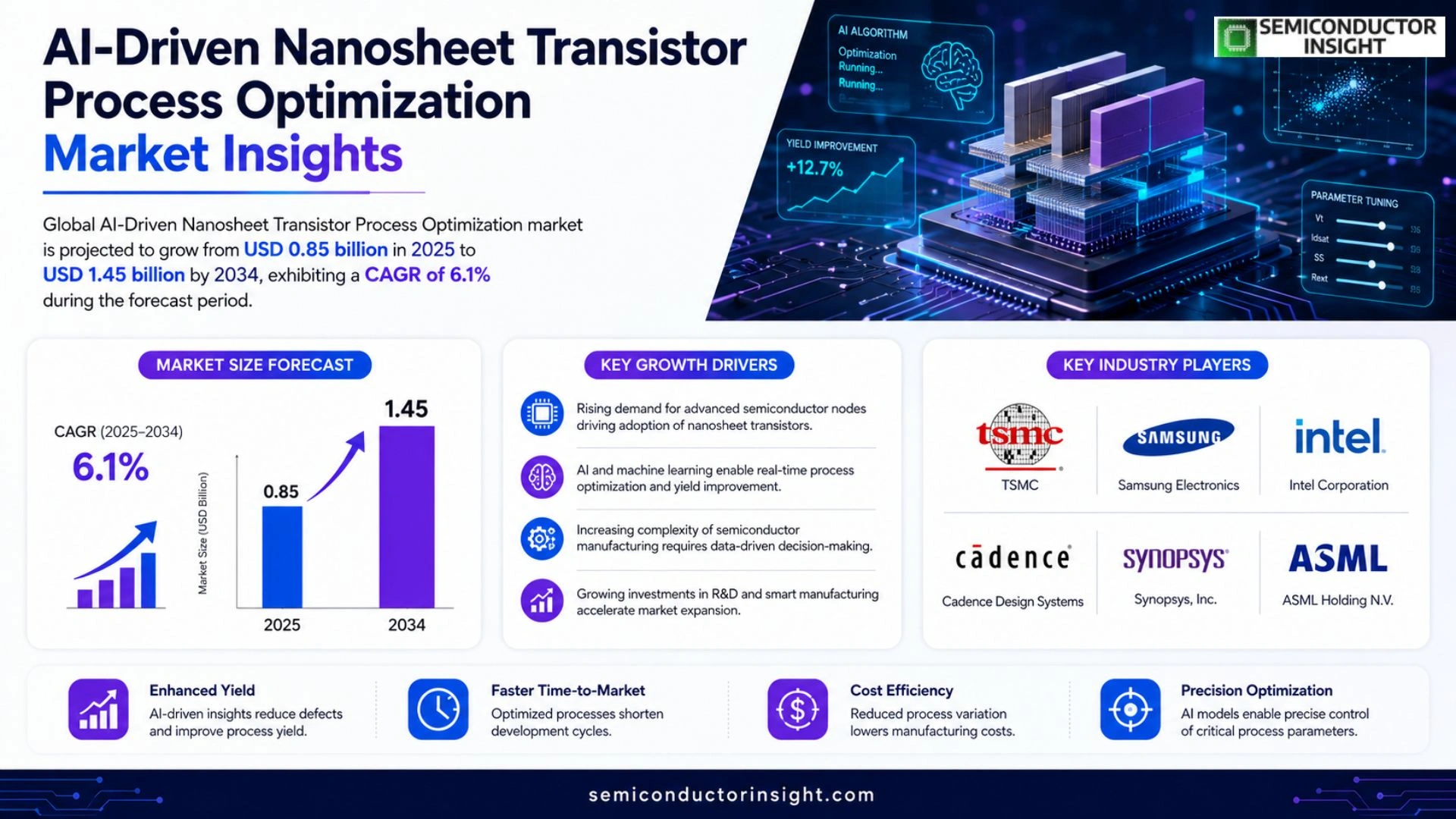
Global AI-Driven Nanosheet Transistor Process Optimization market size was valued at USD 0.85 billion in 2025. The market is projected to grow from USD 0.85 billion in 2025 to USD 1.45 billion by 2034, exhibiting a CAGR of 6.1 % during the forecast period.
AI‑driven nanosheet transistor process optimization involves applying machine‑learning models to refine lithography settings, etch chemistries, and gate‑stack formation for gate‑all‑around (GAA) nanosheets. By linking extensive fab data with device performance outcomes, these tools predict optimal process windows that shorten cycle time and lift yield without relying on manual trial‑and‑error.
The sector is accelerating because leading foundries are advancing below the 3 nm node where conventional rule‑based approaches struggle with variability control. Investments in high‑performance computing enable real‑time feedback loops between design and manufacturing teams. Notably, TSMC partnered with Cadence on AI‑assisted GAA patterning in March 2024, Samsung incorporated predictive process control into its EUV line earlier this year, and Intel launched an AI‑enhanced design‐for‐manufacturability suite in July 2023,each move expanding demand for specialized analytics solutions.
MARKET DRIVERS
Advanced Node Scaling Pressures
The semiconductor industry is scrambling to meet the sub‑10 nm node demands that modern computing workloads impose. As device footprints shrink, conventional lithography encounters physical limits, prompting fabs to explore nanosheet transistor architectures that promise superior electro‑static control. AI‑enhanced process tuning emerges as a decisive lever, enabling engineers to extract marginal gains without extensive mask redesigns.
Data‑Centric Design Methodologies
Design teams are amassing terabytes of measurement data from pilot lines. Machine‑learning models can sift through this volume, identifying subtle pattern shifts that indicate yield loss. By integrating such insights directly into the manufacturing loop, the AI‑Driven Nanosheet Transistor Process Optimization Market gains traction as a cost‑containment tool. Companies that embed these analytics early are likely to outpace peers in time‑to‑volume.
➤ “When AI predicts a 0.3 % variation in gate length before the wafer reaches final inspection, the resulting yield uplift can translate into millions of dollars annually.”
Beyond yield, the ability to accelerate design‑for‑manufacturability cycles shortens product introductions. This agility is crucial as end‑users demand AI accelerators and high‑performance graphics chips with tighter launch windows. Consequently, investment in intelligent process optimization is reshaping capital allocation across the supply chain.
MARKET CHALLENGES
Integration Complexity Across Tool Chains
Deploying AI models within existing fab software stacks demands seamless data exchange between equipment manufacturers, MES systems, and analytics platforms. Misaligned interfaces can erode the anticipated efficiency gains, forcing operators to maintain duplicate workflows. The learning curve associated with cross‑functional integration often outweighs short‑term benefits.
Other Challenges
Talent Scarcity
A limited pool of engineers fluent in both semiconductor physics and advanced AI techniques hampers rapid deployment. Companies must either invest heavily in upskilling programs or compete for scarce specialist talent, both of which exert pressure on project timelines and budgets.
Furthermore, the sensitivity of process data raises concerns around intellectual property protection. Enterprises hesitant to share performance metrics across ecosystems may adopt siloed solutions, diminishing the collective learning advantage that AI promises.
MARKET RESTRAINTS
High Capital Expenditure Threshold
Implementing AI‑driven optimization requires not only software licenses but also significant upgrades to data acquisition hardware. For midsize fabs, the upfront investment can strain balance sheets, leading to delayed adoption cycles. This financial hurdle tempers the overall market pace.
The return horizon for AI projects in nanosheet processes is often multi‑year, given the iterative nature of model refinement and validation. Stakeholders seeking quicker payback may prioritize incremental process tweaks over transformative AI solutions, further restraining market breadth.
Regulatory scrutiny around automated decision‑making in critical manufacturing steps adds another layer of caution. Compliance audits and validation protocols extend deployment timelines, nudging some operators toward proven, manual optimization routes.
MARKET OPPORTUNITIES
Cross‑Industry Collaboration Platforms
Emerging consortia that pool anonymized process data across competing fabs present an avenue for accelerated model training. Participants stand to benefit from shared insights without compromising proprietary details, unlocking a collaborative edge that could reshape the AI‑Driven Nanosheet Transistor Process Optimization Market.
Another fertile ground lies in the integration of edge‑computing capabilities directly on fab equipment. By processing sensor streams locally, latency drops dramatically, enabling real‑time corrective actions that were previously impossible with cloud‑centric analytics.
Finally, the push toward sustainability is motivating fabs to reduce waste and energy consumption. AI solutions that fine‑tune etch and deposition steps can lower chemical usage, aligning cost savings with environmental objectives and opening new funding streams from green‑technology incentives.
AI-Driven Nanosheet Transistor Process Optimization Market Trends
Integration of AI at the Sub‑3 nm Node
The shift to sub‑3 nm gate‑all‑around architectures has exposed the limits of static rule sets that once guided lithography and etch steps. By embedding machine‑learning models directly into the fab workflow, manufacturers now extract actionable insights from terabytes of process telemetry. This capability trims the number of experimental runs required to lock‑in a stable process window, translating into faster time‑to‑volume for advanced nodes. The change is not merely technological; it reshapes resource allocation, as data‑science teams grow alongside traditional process engineers, creating a hybrid talent pool that can react to variability in real time.
Other Trends
Strategic Partnerships Accelerate Solution Adoption
Recent collaborations illustrate how ecosystem players are capitalising on AI‑enabled optimisation. In March 2024, TSMC announced a joint effort with Cadence to embed predictive analytics within its GAA patterning flow, allowing designers to receive process feedback during layout creation. Samsung’s integration of a predictive control module into its EUV production line earlier this year reduced mask‑defect rates by a measurable margin, while Intel’s July 2023 launch of an AI‑enhanced design‑for‑manufacturability suite provided a seamless bridge between circuit intent and fab execution. These alliances not only broaden the addressable market but also set a benchmark for interoperability across toolchains.
Emergence of Real‑Time Feedback Loops
High‑performance computing clusters now sit at the heart of process optimisation loops, crunching sensor data every few seconds to recalibrate exposure doses or etch chemistries. The immediate impact is a noticeable lift in yield consistency, especially for devices whose performance hinges on tight dimensional control. From a business perspective, the reduction in scrap and re‑work translates into cost avoidance that outweighs the upfront investment in AI infrastructure. Moreover, the ability to forecast process drift empowers supply‑chain planners to align wafer inventories with projected demand more accurately, mitigating the risk of over‑production.
COMPETITIVE LANDSCAPE
Key Industry Players
AI‑Driven Nanosheet Transistor Process Optimization: Competitive Overview
The market is currently anchored by a handful of integrated device manufacturers that combine advanced GAA process capability with in‑house AI analytics. TSMC, leveraging its partnership with Cadence, has operationalized a closed‑loop optimization platform that directly correlates lithography variables with device yield, effectively shortening the development cycle for sub‑3 nm products. Samsung’s EUV line integrates predictive process control modules supplied by its silicon‑photonic group, allowing rapid adjustment of etch chemistry without manual re‑tuning. Intel’s recent launch of an AI‑enhanced design‑for‑manufacturability suite demonstrates a strategic move to embed machine‑learning insights across the product stack, strengthening its position against the foundry leaders. The combined influence of these three players creates a tiered structure where the leading foundries dictate the pace of tool adoption, while specialist EDA firms such as Cadence and Synopsys focus on algorithmic differentiation and licensing models.
Beyond the dominant trio, a coalition of equipment and metrology suppliers is shaping the ecosystem through targeted AI functionalities. ASML’s next‑generation EUV tools incorporate real‑time pattern‑recognition to curb stochastic defects, while Applied Materials and Lam Research embed process‑prediction models within deposition and etch modules, respectively. KLA’s inspection platforms now deliver anomaly‑detection scores that feed directly into fab‑wide optimization loops. GlobalFoundries, Tokyo Electron, and NXP Semiconductors are investing in proprietary data‑pipeline infrastructure to tap into the same machine‑learning benefits, albeit at a smaller scale. These niche participants broaden the competitive landscape, offering customers a menu of plug‑in solutions that can be mixed and matched to suit specific node targets or volume requirements.
List of Key AI‑Driven Nanosheet Transistor Process Optimization Companies Profiled
- TSMC
- Samsung Electronics
- Intel Corporation
- Cadence Design Systems
- Synopsys, Inc.
- ASML Holding N.V.
- Applied Materials, Inc.
- KLA Corporation
- Lam Research Corporation
- GlobalFoundries Inc.
- Tokyo Electron Limited
- NXP Semiconductors N.V.
- Mentor, a Siemens Business
- IBM Research (AI Analytics Division)
- Qualcomm Technologies, Inc.
Segment Analysis:
| Segment Category | Sub-Segments | Key Insights |
| By Type |
|
AI‑Enhanced Process Type
|
| By Application |
|
Yield‑Driven Application
|
| By End User |
|
Foundry‑Centric Segment
|
| By Technology |
|
GAA‑Focused Technology
|
| By Process Stage |
|
Patterning Stage Leadership
|
Regional Analysis: AI-Driven Nanosheet Transistor Process Optimization Market
Proprietary AI models are emerging from research labs that blend reinforcement learning with process physics, enabling predictive adjustments before a wafer enters the chamber. Partnerships between AI firms and fabs accelerate knowledge transfer, shortening the latency between algorithm development and production deployment.
The need for high‑bandwidth data links and edge compute nodes is reshaping the supply chain, prompting fabs to source specialized processors that can handle terabytes of sensor output without adding latency to the process flow.
Policymakers have adopted a technology‑agnostic stance, focusing on data integrity and cybersecurity rather than prescribing specific AI techniques, granting manufacturers flexibility to explore novel optimization pathways.
Chip designers are increasingly demanding wafer‑level AI insights to validate design corners early, driving fabs to bundle optimization services with traditional manufacturing agreements.
Europe
European fabs benefit from a strong emphasis on precision engineering and a well‑established standards framework. Collaborative research initiatives across the EU encourage cross‑border sharing of AI algorithms, which helps manufacturers harmonize process parameters across multiple sites. While capital availability is more conservative than in North America, the region’s focus on sustainability pushes firms to adopt AI solutions that reduce material waste and energy consumption, creating a niche advantage for environmentally conscious customers.
Asia‑Pacific
The Asia‑Pacific region is witnessing rapid expansion of advanced node facilities, particularly in Taiwan, South Korea, and China. Local governments are investing heavily in AI‑enabled semiconductor parks, offering tax incentives for companies that embed machine‑learning workflows into their production lines. Talent pipelines are bolstered by large engineering cohorts, yet the challenge lies in aligning disparate AI standards across jurisdictions, which could affect the speed of cross‑regional technology diffusion.
South America
South America remains an emerging participant, with Brazil leading modest pilot projects that integrate AI for defect detection in older node fabs. Market entry barriers include limited access to high‑performance compute resources and a fragmented supply chain, but strategic partnerships with North American AI vendors are beginning to close the capability gap, suggesting a gradual upward trajectory.
Middle East & Africa
In the Middle East & Africa, nascent semiconductor initiatives are being supported by sovereign wealth funds that view AI‑enabled manufacturing as a diversification strategy. Pilot programs in the United Arab Emirates focus on using AI for process monitoring in research‑scale fabs, while African investments are still exploratory, concentrating on building foundational talent and infrastructure before scaling to commercial production.
Report Scope
This market research report provides a comprehensive analysis of the AI-Driven Nanosheet Transistor Process Optimization Market , covering the forecast period 2026–2034. It offers detailed insights into market dynamics, technological advancements, competitive landscape, and key trends shaping the industry.
Key focus areas of the report include:
- Market Overview: The report begins with an overview outlining its current market scenario, key growth indicators, and industry transformation drivers. It discusses macroeconomic factors, demand–supply balance, regulatory landscape, and the strategic role of semiconductors in powering advancements across industries such as automotive, telecommunications, consumer electronics, and industrial automation.
- Market Size & Forecast: Historical data and future projections for revenue, unit shipments, and market value across major regions and segments.
- Segmentation Analysis: Detailed breakdown by product type, technology, application, and end-user industry to identify high-growth segments and investment opportunities.
- Regional Insights: Insights into market performance across North America, Europe, Asia‑Pacific, Latin America, and the Middle East & Africa, including country-level analysis where relevant.
- Competitive Landscape: Profiles of leading market participants, including their product offerings, R&D focus, manufacturing capacity, pricing strategies, and recent developments such as mergers, acquisitions, and partnerships.
- Technology Trends & Innovation: Assessment of emerging technologies, integration of AI/IoT, semiconductor design trends, fabrication techniques, and evolving industry standards.
- Market Drivers & Restraints: Evaluation of factors driving market growth along with challenges, supply chain constraints, regulatory issues, and market-entry barriers.
- Stakeholder Insights: Insights for component suppliers, OEMs, system integrators, investors, and policymakers regarding the evolving ecosystem and strategic opportunities.
Primary and secondary research methods are employed, including interviews with industry experts, data from verified sources, and real-time market intelligence to ensure the accuracy and reliability of the insights presented.
FREQUENTLY ASKED QUESTIONS:
What is the current market size of AI-Driven Nanosheet Transistor Process Optimization Market?
-> AI-Driven Nanosheet Transistor Process Optimization market size was valued at USD 1.45 billion by 2034, exhibiting a CAGR of 6.1 % during the forecast period.
Which key companies operate in AI-Driven Nanosheet Transistor Process Optimization Market?
-> Key players include TSMC, Cadence, Samsung, Intel, among others.
What are the key growth drivers?
-> Key growth drivers include advancement of sub‑3 nm nodes, high‑performance computing integration, and demand for yield‑enhancing AI analytics.
Which region dominates the market?
-> Asia‑Pacific leads due to major semiconductor fabs, while North America shows strong adoption of AI‑driven process solutions.
What are the emerging trends?
-> Emerging trends include AI‑assisted GAA patterning, predictive EUV control, and AI‑enhanced design‑for‑manufacturability suites.

Get Sample Report PDF for Exclusive Insights
Report Sample Includes
- Table of Contents
- List of Tables & Figures
- Charts, Research Methodology, and more...
 Download Sample Report PDF




