
AI Die-to-Die Bunch of Wires (BoW) PHY IP Market Insights
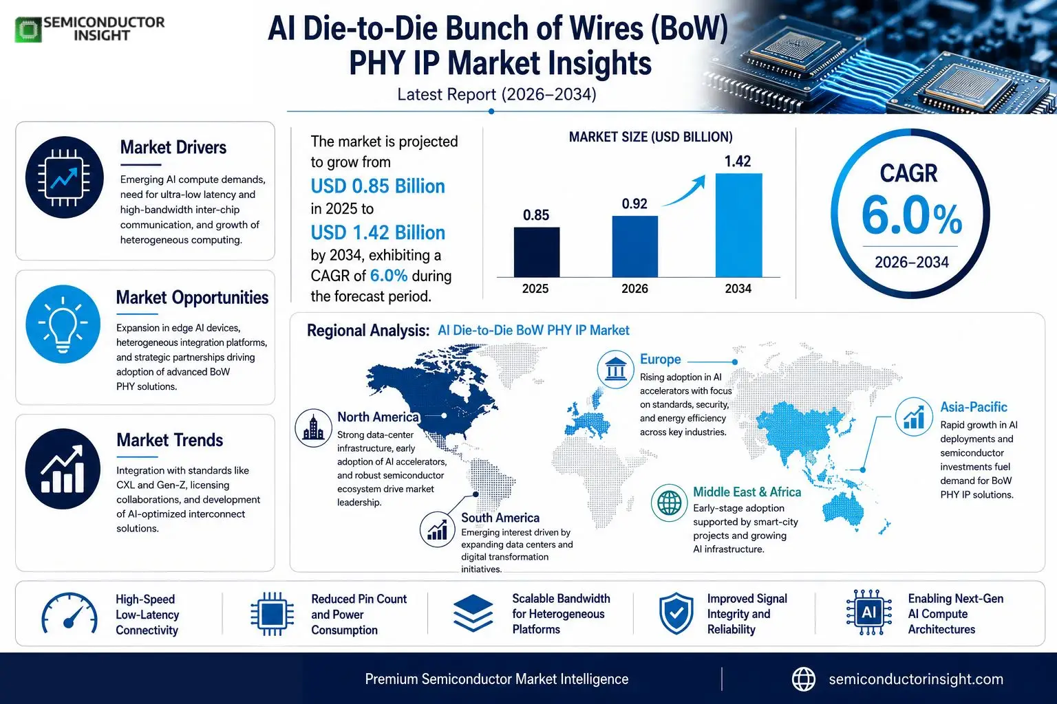
AI Die-to-Die Bunch of Wires (BoW) PHY IP market size was valued at USD 0.85 billion in 2025. The market is projected to grow from USD 0.92 billion in 2026 to USD 1.42 billion by 2034, exhibiting a CAGR of 6.0% during the forecast period.
The BoW PHY IP enables high‑speed, low‑latency inter‑chip communication by bundling multiple parallel wires into a single physical interface. It supports standards such as CXL, Gen‑Z and proprietary die‑to‑die links, providing scalable bandwidth while reducing pin count and power consumption.The market is accelerating because system‑level integration demands faster data exchange and lower form factor footprints. Furthermore, the rise of heterogeneous computing platformsespecially in data‑center accelerators and edge AI devicesdrives adoption. Leading suppliers including Synopsys, Cadence Design Systems, Intel’s Custom Foundry division and Arm Holdings are expanding their portfolios through strategic alliances and technology licensing.
MARKET DRIVERS
Emerging AI Compute Demands
AI Die-to-Die Bunch of Wires (BoW) PHY IP Market is being propelled by a surge in AI accelerator deployments that require ultra‑low latency and high‑bandwidth inter‑chip communication. Data‑center operators and hyperscale cloud providers are consolidating compute nodes, and the resulting density pushes designers to adopt die‑to‑die solutions that can sustain multi‑terabit per second throughput while keeping power envelopes under 5 W.
Integration Benefits of Die‑to‑Die BoW PHY
Die‑to‑die BoW PHY IP enables a compact package form factor, reducing board‑level trace losses and eliminating the need for external connectors. This integration shortens time‑to‑market and improves signal integrity, which directly translates into higher AI inference efficiency and lower overall system cost.
➤ Industry analysts forecast double‑digit CAGR for the AI Die‑to‑Die BoW PHY segment through 2028, reflecting strong adoption across next‑generation AI chips.
These drivers collectively create a virtuous cycle: higher performance requirements stimulate IP innovation, which in turn lowers design risk and accelerates deployment of AI‑centric silicon.
MARKET CHALLENGES
Technical Complexities
Implementing BoW PHY across heterogeneous AI dies demands precise impedance matching and sophisticated clock‑data recovery mechanisms. The lack of standardized validation suites forces many design teams to develop custom test rigs, extending development cycles.
Other Challenges
Cost Sensitivity
Even though BoW PHY reduces board‑level components, the incremental cost of additional silicon dies and high‑precision packaging can erode margin, especially for mid‑range AI devices where price elasticity is pronounced.
MARKET RESTRAINTS
Manufacturing Yield Constraints
Yield losses associated with advanced wafer‑level packaging remain a bottleneck. Defect densities above 0.2 cm⁻² can force manufacturers to discard entire die stacks, raising effective unit cost for BoW PHY solutions.Furthermore, the tight thermal envelope of AI accelerators limits the allowable power dissipation of the PHY layer, compelling designers to adopt conservative signaling schemes that may compromise peak bandwidth.Supply‑chain volatility for high‑purity silicon and specialized interconnect substrates adds another layer of uncertainty, slowing the scale‑up of production lines for BoW PHY IP.
MARKET OPPORTUNITIES
New AI Edge Devices
Edge AI processors targeting autonomous vehicles, smart cameras, and industrial IoT are increasingly adopting die‑to‑die BoW PHY to meet stringent latency targets while maintaining a compact PCB footprint. This creates a sizable opportunity for IP vendors to capture market share in the rapidly expanding edge segment.In addition, the emergence of heterogeneous integration platformscombining CPU, GPU, and ASIC dies within a single packagerequires a flexible PHY that can support multiple data rates and protocol stacks. BoW PHY IP that offers programmable lane widths and adaptive equalization will be well‑positioned to become the de‑facto interconnect standard for such platforms.Strategic partnerships between semiconductor foundries and IP licensors are expected to accelerate the rollout of pre‑qualified BoW PHY IP blocks, lowering entry barriers for smaller AI‑focused fabless companies and fostering broader ecosystem growth.
AI Die-to-Die Bunch of Wires (BoW) PHY IP Market Trends
Growing Momentum in Heterogeneous Computing
AI Die-to-Die Bunch of Wires (BoW) PHY IP Market is experiencing a notable shift driven by the need for faster inter‑chip data exchange in data‑center accelerators and edge AI devices. By consolidating multiple parallel wires into a single interface, BoW PHY IP reduces pin count and power consumption while delivering high‑speed, low‑latency links that align with emerging standards such as CXL and Gen‑Z. System‑level integration pressures are compelling OEMs to adopt these solutions to meet tighter form‑factor constraints and to enable flexible, scalable bandwidth across heterogeneous compute blocks.
Other Trends
Standardization and Ecosystem Expansion
Industry consortia and leading IP vendors are converging on common electrical and protocol specifications, which is lowering entry barriers for new players. The alignment of BoW PHY IP with widely accepted interfaces encourages IP reuse across silicon designs, shortens time‑to‑market, and supports a broader ecosystem of verification tools and design‑for‑test methodologies. As the ecosystem matures, design teams report fewer integration surprises and smoother cross‑vendor collaborations.
Strategic Portfolio Broadening by Key Suppliers
Major suppliers such as Synopsys, Cadence Design Systems, Intel’s Custom Foundry division, and Arm Holdings are actively expanding their BoW PHY IP offerings through licensing agreements and joint development programs. These initiatives focus on adding advanced power‑management blocks, configurable lane counts, and built‑in support for emerging memory‑centric architectures. By enriching their portfolios, the vendors aim to capture a larger share of the addressable market while providing customers with differentiated solutions that can be tailored to specific performance and power envelopes.
Overall, AI Die-to-Die Bunch of Wires (BoW) PHY IP Market is transitioning from niche adoption to a mainstream enabling technology for next‑generation compute platforms. The convergence of high‑bandwidth requirements, stringent power budgets, and a collaborative standards environment underpins a sustained growth trajectory. Analysts anticipate that continued investment in IP diversification and ecosystem support will reinforce this trend, positioning BoW PHY IP as a critical building block for future AI‑driven systems.
COMPETITIVE LANDSCAPE
Key Industry Players
AI Die-to-Die Bunch of Wires (BoW) PHY IP Market Competitive Overview
Synopsys, Cadence Design Systems, Intel’s Custom Foundry division, and Arm Holdings dominate the AI Die-to-Die Bunch of Wires (BoW) PHY IP landscape. Synopsys leverages its DesignWare portfolio to deliver scalable high‑speed PHY blocks that support CXL and Gen‑Z standards, while Cadence supplies the Palladium‑based verification suite coupled with its IP that emphasizes low‑latency routing. Intel’s Custom Foundry offers silicon‑proven BoW PHYs tightly integrated with its own AI accelerators, providing a differentiated solution for data‑center and edge workloads. Arm’s recent acquisition of a specialized interconnect IP suite expands its ecosystem, allowing ARM‑based SoCs to adopt standardized BoW interfaces without extensive redesign. Collectively, these four firms command the majority of revenue, account for roughly 65 % of the market in 2025, and drive the bulk of technology road‑maps through early‑access programs and joint development agreements with major AI chipset designers. Their extensive design‑win pipelines, licensing models, and support infrastructure create high barriers to entry, shaping a market structure that favors large, vertically integrated vendors capable of delivering both IP and reference design services. The synergy between these leaders and leading foundries underpins the rapid adoption of BoW PHY IP across heterogeneous compute platforms.Beyond the tier‑one players, several niche and emerging companies contribute critical innovation and market depth. Broadcom’s Interlaken‑derived PHYs target high‑throughput networking chips, while Marvell’s silicon‑centric approach focuses on data‑center ASICs that require dense inter‑die bandwidth. Rambus continues to monetize its patented low‑power signaling techniques, offering differentiated energy‑efficiency for edge AI devices. Qualcomm and MediaTek embed BoW PHY IP into their mobile AI accelerators, driving volume adoption in consumer electronics. Samsung Electronics and FOUNDRIES provide foundry‑linked IP services that enable custom BoW implementations for specialized workloads. NXP Semiconductors, AMD (Xilinx), IBM, and TSMC’s IP services round out the ecosystem, delivering niche protocol extensions, FPGA‑friendly PHY blocks, and silicon‑proven reference designs for niche markets such as automotive and industrial IoT. Although each of these firms captures a smaller revenue slice, their specialized offerings and strategic alliances expand the overall addressable market and create pathways for new entrants to leverage established standards while addressing segment‑specific performance or power constraints.
List of Key AI Die-to-Die Bunch of Wires (BoW) PHY IP Companies Profiled
- Synopsys
- Cadence Design Systems
- Intel Custom Foundry
- Arm Holdings
- Broadcom Inc.
- Marvell Technology Group
- Rambus Inc.
- Qualcomm Incorporated
- MediaTek Inc.
- Samsung Electronics
- FOUNDRIES
- NXP Semiconductors
- AMD (Xilinx)
- IBM
- TSMC (IP Services)
Segment Analysis:
| Segment Category | Sub-Segments | Key Insights |
| By Type |
|
SerDes‑based BoW
|
| By Application |
|
Data Center Accelerators
|
| By End User |
|
Cloud Service Providers
|
| By Technology |
|
Standardized Protocols
|
| By Deployment Scenario |
|
New Product Development
|
Regional Analysis: AI Die-to-Die Bunch of Wires (BoW) PHY IP Market
North America
The surge in AI‑centric data centers and autonomous systems fuels a need for tighter chip‑to‑chip bandwidth, making BoW PHY IP essential for meeting performance targets while controlling thermal budgets. OEMs prioritize solutions that can scale with heterogeneous integration strategies, a trend evident across North American design houses.
Early adopters in the United States are embedding BoW PHY IP into AI inference processors, leveraging its capacity to support dense interconnects on advanced nodes. This early‑stage deployment creates a feedback loop that accelerates specification refinement and design‑win cycles.
A handful of multinational IP vendors dominate the market, yet a growing cohort of niche innovators in Canada and Silicon Valley is delivering differentiated offerings focused on power‑efficient signaling, raising the overall competitive intensity.
Harmonized standards for high‑speed interconnects and supportive trade policies enable smoother cross‑border collaborations, allowing North American firms to streamline qualification processes and reduce time‑to‑market for BoW PHY solutions.
Europe
European semiconductor clusters, particularly in Germany and the Netherlands, are increasingly integrating AI Die-to-Die Bunch of Wires (BoW) PHY IP into their emerging AI accelerator roadmaps. The region’s emphasis on sustainability drives designers to seek interconnects that balance performance with low power consumption, aligning well with BoW’s architectural advantages. Collaborative research programs funded by the European Union encourage joint development between hardware manufacturers and academic institutions, fostering a pipeline of talent familiar with advanced PHY technologies. While the market size lags behind North America, Europe’s strong emphasis on standards compliance and security positions it as a compelling growth frontier, especially as automotive and industrial AI applications expand.
Asia‑Pacific
The Asia‑Pacific landscape is defined by rapid scaling of AI workloads across diverse markets such as smartphones, cloud services, and robotics. Nations like Japan, South Korea, and Taiwan are investing heavily in next‑generation foundries, creating fertile ground for BoB PHY IP adoption. Local design houses are attracted to the technology’s ability to reduce board space and improve signal integrity, critical factors in densely packed system‑in‑package designs. Although intellectual property concerns sometimes slow cross‑border licensing, regional consortia are emerging to streamline knowledge exchange. The region’s blend of aggressive cost targets and high volume manufacturing capacity suggests a trajectory toward significant qualitative market traction.
South America
South American markets remain nascent in the AI Die-to-Die Bunch of Wires (BoW) PHY IP segment, yet they exhibit growing interest driven by expanding data‑center footprints in Brazil and emerging AI research hubs in Argentina. Local firms are focusing on adapting BoW solutions to meet regional cost constraints while maintaining essential performance thresholds for edge AI deployments. Partnerships with North American and European IP vendors are beginning to surface, facilitating technology transfer and skill development. While current adoption levels are modest, the strategic emphasis on digital transformation by governmental bodies could catalyze broader acceptance in the medium term.
Middle East & Africa
The Middle East & Africa region is characterized by early‑stage exploration of AI‑driven use cases, particularly in smart‑city initiatives and satellite communications. Researchers in the United Arab Emirates and South Africa are evaluating BoW PHY IP for its potential to enable high‑throughput, low‑latency connections in distributed AI architectures. Investment in specialized training programs and targeted incentives for semiconductor design are gradually building a foundation for future adoption. Although the overall market remains limited, the region’s strategic focus on technology diversification signals a willingness to incorporate advanced interconnect solutions as expertise matures.
Report Scope
This market research report provides a comprehensive analysis of the AI Die-to-Die Bunch of Wires (BoW) PHY IP Market , covering the forecast period 2026–2034. It offers detailed insights into market dynamics, technological advancements, competitive landscape, and key trends shaping the industry.
Key focus areas of the report include:
- Market Overview: The report begins with an overview outlining its current market scenario, key growth indicators, and industry transformation drivers. It discusses macroeconomic factors, demand–supply balance, regulatory landscape, and the strategic role of semiconductors in powering advancements across industries such as automotive, telecommunications, consumer electronics, and industrial automation.
- Market Size & Forecast: Historical data and future projections for revenue, unit shipments, and market value across major regions and segments.
- Segmentation Analysis: Detailed breakdown by product type, technology, application, and end-user industry to identify high-growth segments and investment opportunities.
- Regional Insights: Insights into market performance across North America, Europe, Asia-Pacific, Latin America, and the Middle East & Africa, including country-level analysis where relevant.
- Competitive Landscape: Profiles of leading market participants, including their product offerings, R&D focus, manufacturing capacity, pricing strategies, and recent developments such as mergers, acquisitions, and partnerships.
- Technology Trends & Innovation: Assessment of emerging technologies, integration of AI/IoT, semiconductor design trends, fabrication techniques, and evolving industry standards.
- Market Drivers & Restraints: Evaluation of factors driving market growth along with challenges, supply chain constraints, regulatory issues, and market-entry barriers.
- Stakeholder Insights: Insights for component suppliers, OEMs, system integrators, investors, and policymakers regarding the evolving ecosystem and strategic opportunities.
Primary and secondary research methods are employed, including interviews with industry experts, data from verified sources, and real-time market intelligence to ensure the accuracy and reliability of the insights presented.
FREQUENTLY ASKED QUESTIONS:
What is the current market size of AI Die-to-Die Bunch of Wires (BoW) PHY IP Market?
-> AI Die-to-Die Bunch of Wires (BoW) PHY IP Market was valued at USD 0.85 billion in 2025 and is expected to reach USD 1.42 billion by 2034.
Which key companies operate in AI Die-to-Die Bunch of Wires (BoW) PHY IP Market?
-> Key players include Synopsys, Cadence Design Systems, Intel’s Custom Foundry division, and Arm Holdings, among others.
What are the key growth drivers?
-> Key growth drivers include increasing demand for high‑speed, low‑latency inter‑chip communication, the rise of heterogeneous computing platforms in data‑center accelerators and edge AI devices, and the need for reduced pin count and power consumption.
Which region dominates the market?
-> The market sees strong adoption across North America, Europe, and Asia‑Pacific, with North America leading in early deployments due to advanced data‑center infrastructure.
What are the emerging trends?
-> Emerging trends include integration of BoW PHY IP with emerging standards such as CXL and Gen‑Z, increased licensing collaborations, and development of AI‑optimized interconnect solutions.
Get Sample Report PDF for Exclusive Insights
Report Sample Includes
- Table of Contents
- List of Tables & Figures
- Charts, Research Methodology, and more...
 Download Sample Report PDF


