AI CVD Chamber Cleaning Endpoint Optical Emission Spectroscopy Processor Market Insights
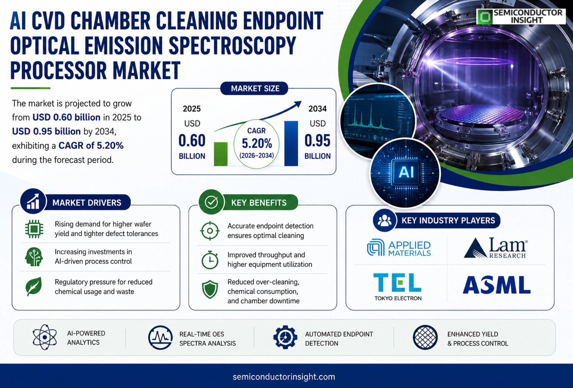
Global AI CVD Chamber Cleaning Endpoint Optical Emission Spectroscopy Processor market size was valued at USD 0.60 billion in 2025. The market is projected to grow from USD 0.60 billion in 2025 to USD 0.95 billion by 2034, exhibiting a CAGR of 5.20% during the forecast period.
The processor combines artificial‑intelligence analytics with optical emission spectroscopy (OES) to determine the precise cleaning endpoint of chemical‑vapor‑deposition (CVD) chambers used in semiconductor fabrication. By interpreting real‑time plasma spectra it predicts residual film thickness and automatically terminates the cleaning cycle.
The market is experiencing rapid growth because semiconductor manufacturers are pushing higher wafer‑per‑hour yields while tightening defect tolerances. Investments in AI‑driven process control, expanding adoption of advanced node technologies, and regulatory pressure for reduced chemical waste are further accelerating demand. Key players such as Applied Materials, Lam Research, Tokyo Electron and ASML are broadening their portfolios with AI‑enabled OES solutions, reinforcing overall market expansion.
MARKET DRIVERS
Increasing Automation in Semiconductor Manufacturing
AI CVD Chamber Cleaning Endpoint Optical Emission Spectroscopy Processor Market is being propelled by a surge in automation across wafer fabrication lines. Manufacturers are adopting artificial‑intelligence algorithms to reduce cycle time, improve yield, and lower total cost of ownership. Real‑time optical emission data enables predictive cleaning, which directly supports higher throughput and tighter defect control.
Advancements in Optical Emission Spectroscopy Accuracy
Recent breakthroughs in spectrometer design have increased detection sensitivity by over 30 %, allowing processors to identify trace contaminants that previously evaded conventional sensors. This heightened accuracy creates a compelling value proposition for fabs aiming to meet sub‑10 nm node specifications, where even minor residues can cause critical failures.
➤ Industry analysts project that AI‑enhanced endpoint detection will be a standard feature in more than 70 % of new CVD tools installed after 2025.
Overall, the convergence of AI‑driven analytics, improved spectroscopy, and the relentless push for smaller geometry nodes establishes a robust growth foundation for the market.
MARKET CHALLENGES
Integration Complexity with Legacy CVD Systems
Many fabs operate a heterogeneous mix of equipment ages, and retrofitting older CVD chambers with the latest AI processors requires extensive hardware redesign and software harmonization. This integration effort can extend shutdown periods, temporarily reducing production capacity.
Other Challenges
Cost of Implementation
The upfront investment for high‑performance optical emission spectrometers, coupled with AI licensing fees, raises capital requirements. Smaller foundries may struggle to justify the expense without clear short‑term ROI evidence.
MARKET RESTRAINTS
High Capital Expenditure for AI‑Enabled Hardware
Purchasing and installing AI‑driven processors demand significant financial outlay, including sensor modules, edge computing units, and specialized cooling systems. The high cost can deter investment, especially in regions where semiconductor subsidies are limited.
MARKET OPPORTUNITIES
Emerging Demand from 3‑nm Node Production
As leading manufacturers transition to 3‑nm and beyond, the tolerance for contaminant‑induced defects narrows dramatically. AI CVD Chamber Cleaning Endpoint Optical Emission Spectroscopy Processor Market stands to benefit from contracts aimed at ensuring ultra‑clean chamber environments, creating a sizable opportunity for vendors that can deliver real‑time, AI‑optimized cleaning cycles.
AI CVD Chamber Cleaning Endpoint Optical Emission Spectroscopy Processor Market Trends
Accelerated Adoption of AI‑Driven Cleaning Endpoints
AI CVD Chamber Cleaning Endpoint Optical Emission Spectroscopy Processor market is witnessing a swift shift toward fully integrated, AI‑enabled process control solutions. By coupling advanced optical emission spectroscopy with real‑time machine‑learning algorithms, these processors can predict residual film thickness and automatically halt the cleaning cycle, eliminating over‑cleaning and reducing cycle time. Semiconductor fabs are prioritizing higher wafer‑per‑hour yields, and the precision offered by AI‑driven endpoints aligns directly with tighter defect tolerances. The technology also supports advanced node production, where marginal variations in chamber contamination can translate into critical yield losses. Consequently, manufacturers are investing heavily in retrofitting existing OES equipment with AI modules and prioritizing new platform purchases that embed these capabilities from the design stage.
Other Trends
Integration with Sustainable Manufacturing Practices
Environmental regulations and corporate sustainability goals are driving demand for processors that minimize chemical waste. AI CVD Chamber Cleaning Endpoint Optical Emission Spectroscopy Processor reduces unnecessary reagent exposure by accurately identifying the exact cleaning point, which in turn lowers waste disposal costs and chemical consumption. Major equipment vendors such as Applied Materials, Lam Research, Tokyo Electron, and ASML are expanding their portfolios to include AI‑optimized OES solutions that report waste metrics in real time, enabling fabs to demonstrate compliance with tightening emissions standards. This focus on waste reduction is becoming a differentiator for suppliers, prompting collaborative development programs between semiconductor manufacturers and processor developers to fine‑tune algorithms for specific process chemistries.
Strategic Partnerships and Ecosystem Expansion
Beyond individual product development, the market is shaped by strategic alliances that bring together AI software firms, spectroscopy hardware specialists, and fab service providers. These partnerships accelerate the rollout of turnkey solutions, allowing fabs to adopt AI CVD Chamber Cleaning Endpoint Optical Emission Spectroscopy Processor with minimal integration risk. Collaborative roadmaps are emphasizing modular firmware updates, cloud‑based analytics dashboards, and standardized data interfaces, which together create a scalable ecosystem for continuous improvement. As the industry consolidates around these interoperable platforms, the overall market trajectory remains firmly upward, powered by the combined forces of technological innovation, sustainability imperatives, and cross‑industry collaboration.
COMPETITIVE LANDSCAPE
Key Industry Players
AI‑Driven OES Processors Transform CVD Chamber Cleaning
AI CVD Chamber Cleaning Endpoint Optical Emission Spectroscopy (OES) Processor market is dominated by a small group of large equipment manufacturers that leverage deep semiconductor expertise and AI analytics platforms. Applied Materials, Lam Research, Tokyo Electron and ASML lead the market by integrating proprietary AI models with high‑resolution OES sensors, enabling real‑time plasma‑spectra interpretation and automatic cycle termination. Their extensive service networks and close partnerships with fab customers create high entry barriers, while their product portfolios span multiple process nodes, reinforcing a consolidated competitive structure that favors scale, data richness, and software‑as‑a‑service offerings.
Beyond the tier‑one leaders, a diverse set of niche innovators contributes specialized capabilities that enrich the ecosystem. KLA Corporation supplies advanced metrology and defect inspection tools that complement OES data streams, while Hitachi High‑Technologies and Advantest focus on precision spectrometer hardware. Companies such as Cymer (now part of ASML), Entegris, Axcelis Technologies, Samsung Electronics, and Intel Corporation are expanding their AI‑enabled process‑control portfolios, creating a layered competitive landscape where differentiated algorithms, sensor precision, and integration with broader fab automation platforms drive market differentiation.
List of Key AI CVD Chamber Cleaning Endpoint Optical Emission Spectroscopy Processor Companies Profiled
- Applied Materials
- Lam Research
- Tokyo Electron
- ASML
- KLA Corporation
- Hitachi High‑Technologies
- Advantest Corporation
- Cymer
- Entegris
- Axcelis Technologies
- Samsung Electronics
- Intel Corporation
Segment Analysis:
| Segment Category | Sub-Segments | Key Insights |
| By Type |
|
AI‑Enabled Spectroscopy Processors are increasingly favored because they translate complex plasma signatures into actionable cleaning decisions, support higher wafer‑per‑hour productivity, and align with sustainability goals.
|
| By Application |
|
Wafer cleaning endpoint detection drives market relevance as fabs demand exact termination of cleaning cycles to protect device integrity while maintaining throughput.
|
| By End User |
|
Semiconductor fab operators are the primary drivers, seeking reliability, rapid insight, and integration ease to sustain high‑volume production.
|
| By Deployment Model |
|
Cloud‑based solutions are gaining traction as they deliver scalable analytics without heavy upfront hardware investment.
|
| By Functional Capability |
|
Real‑time analytics distinguishes leading processors by delivering immediate interpretation of emission spectra, empowering operators to act instantaneously.
|
Regional Analysis: AI CVD Chamber Cleaning Endpoint Optical Emission Spectroscopy Processor Market
The pursuit of sub‑nanometer process control drives demand for AI‑enhanced emission spectroscopy. Makers seek to minimize particle contamination and cycle time, prompting adoption of intelligent cleaning processors that self‑optimize based on real‑time data streams.
Federal safety and environmental guidelines increasingly reference advanced monitoring technologies. Compliance frameworks encourage transparent reporting of chamber conditions, positioning AI spectroscopy as a preferred method for meeting stringent cleanroom standards.
Integration of edge AI chips with optical emission sensors enables on‑device inference, reducing latency. Recent firmware upgrades focus on adaptive learning models that accommodate new precursor chemistries without extensive re‑training.
A handful of specialist firms dominate, but major equipment OEMs are acquiring niche AI vendors to bundle processing capabilities, fostering an increasingly consolidated market structure.
Europe
European semiconductor clusters, particularly in Germany and the Netherlands, are steadily expanding AI‑enabled cleaning solutions. Collaborative research initiatives under the Horizon Europe programme facilitate knowledge exchange between AI developers and CVD equipment makers. Manufacturers value the region’s strong emphasis on sustainability, prompting integration of energy‑efficient processors that align with EU Green Deal objectives. Although regulatory approval processes are rigorous, they provide a clear pathway for technology validation, reinforcing market confidence.
Asia‑Pacific
The Asia‑Pacific region showcases rapid scaling of semiconductor fabs, especially in Taiwan, South Korea, and Singapore. Cost‑sensitive producers are beginning to recognize the long‑term yield benefits of AI spectroscopy, leading to pilot deployments in high‑volume manufacturing. Local government incentives for smart manufacturing accelerate adoption, while partnerships with academic institutions drive algorithmic customization for region‑specific process chemistries.
South America
South American markets are in an early adoption phase, with emerging investments in advanced packaging and display technologies. Regional players are exploring AI cleaning processors to bridge the quality gap with more established competitors. Government initiatives aimed at diversifying manufacturing bases create a conducive environment for technology transfer and skill development in AI‑driven process control.
Middle East & Africa
Growth in the Middle East & Africa is propelled by strategic diversification away from oil‑centric economies toward high‑tech manufacturing. Emerging semiconductor hubs in the United Arab Emirates and South Africa are experimenting with AI CVD chamber solutions to attract multinational fabs. Partnerships with global OEMs provide access to cutting‑edge processors, while local talent development programs nurture the expertise needed for sustained implementation.
Report Scope
This market research report provides a comprehensive analysis of the AI CVD Chamber Cleaning Endpoint Optical Emission Spectroscopy Processor Market , covering the forecast period 2026–2034. It offers detailed insights into market dynamics, technological advancements, competitive landscape, and key trends shaping the industry.
Key focus areas of the report include:
- Market Overview: The report begins with an overview outlining its current market scenario, key growth indicators, and industry transformation drivers. It discusses macroeconomic factors, demand–supply balance, regulatory landscape, and the strategic role of semiconductors in powering advancements across industries such as automotive, telecommunications, consumer electronics, and industrial automation.
- Market Size & Forecast: Historical data and future projections for revenue, unit shipments, and market value across major regions and segments.
- Segmentation Analysis: Detailed breakdown by product type, technology, application, and end-user industry to identify high-growth segments and investment opportunities.
- Regional Insights: Insights into market performance across North America, Europe, Asia-Pacific, Latin America, and the Middle East & Africa, including country-level analysis where relevant.
- Competitive Landscape: Profiles of leading market participants, including their product offerings, R&D focus, manufacturing capacity, pricing strategies, and recent developments such as mergers, acquisitions, and partnerships.
- Technology Trends & Innovation: Assessment of emerging technologies, integration of AI/IoT, semiconductor design trends, fabrication techniques, and evolving industry standards.
- Market Drivers & Restraints: Evaluation of factors driving market growth along with challenges, supply chain constraints, regulatory issues, and market-entry barriers.
- Stakeholder Insights: Insights for component suppliers, OEMs, system integrators, investors, and policymakers regarding the evolving ecosystem and strategic opportunities.
Primary and secondary research methods are employed, including interviews with industry experts, data from verified sources, and real-time market intelligence to ensure the accuracy and reliability of the insights presented.
FREQUENTLY ASKED QUESTIONS:
What is the current market size of AI CVD Chamber Cleaning Endpoint Optical Emission Spectroscopy Processor Market?
-> AI CVD Chamber Cleaning Endpoint Optical Emission Spectroscopy Processor market is projected to grow from USD 0.60 billion in 2025 to USD 0.95 billion by 2034
Which key companies operate in AI CVD Chamber Cleaning Endpoint Optical Emission Spectroscopy Processor Market?
-> Key players include Applied Materials, Lam Research, Tokyo Electron, and ASML, among others.
What are the key growth drivers?
-> Key growth drivers include higher wafer‑per‑hour yields, tighter defect tolerances, AI‑driven process control investments, adoption of advanced node technologies, and regulatory pressure for reduced chemical waste.
Which region dominates the market?
-> Regional dominance is not detailed in the current reference data.
What are the emerging trends?
-> Emerging trends include AI‑enabled optical emission spectroscopy solutions, integration of AI analytics for real‑time cleaning endpoint detection, and adoption of advanced node technologies.
Get Sample Report PDF for Exclusive Insights
Report Sample Includes
- Table of Contents
- List of Tables & Figures
- Charts, Research Methodology, and more...


