
AI Chip Multi-Die Integration EDA Tools Market Insights
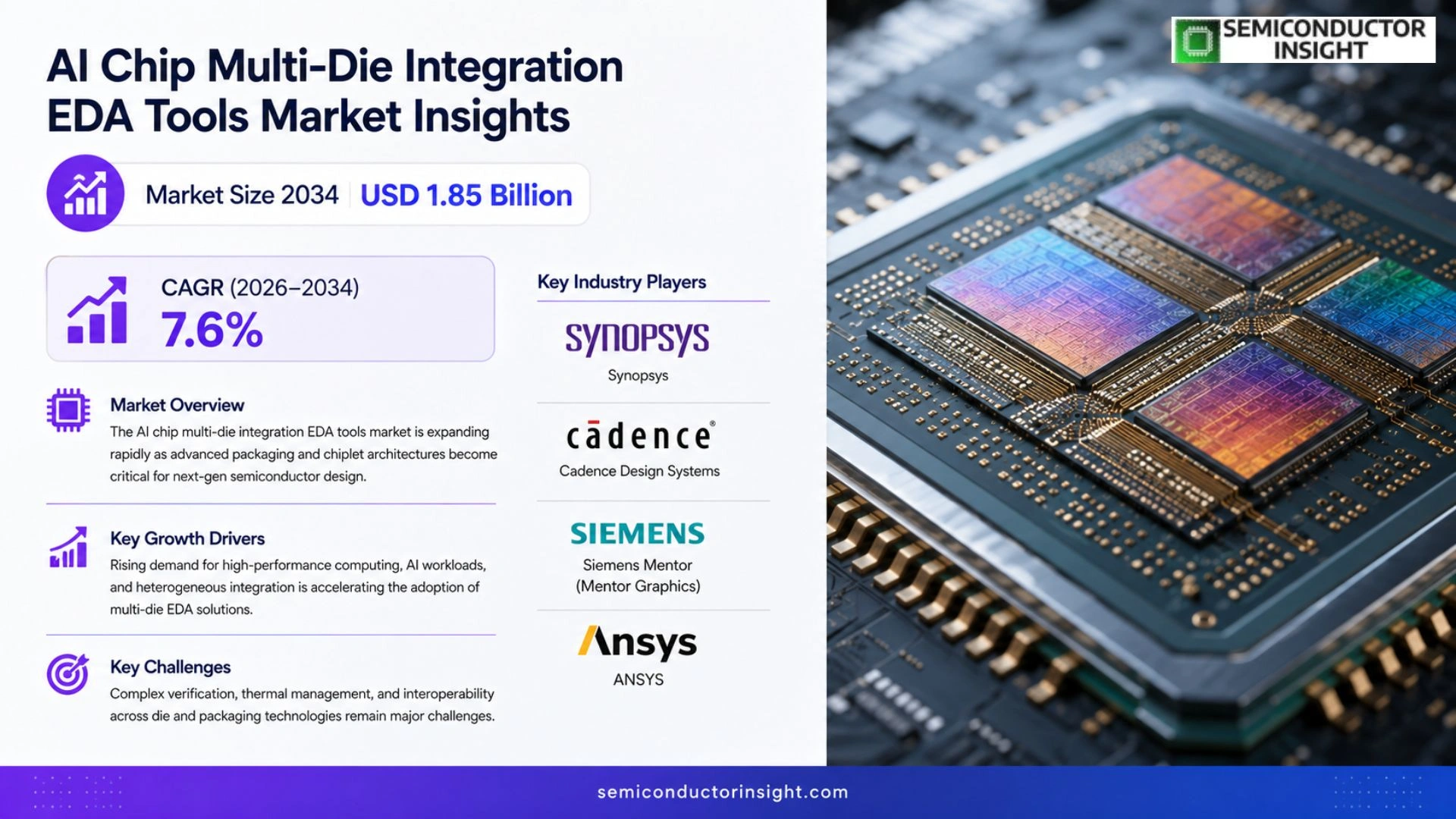
AI Chip Multi-Die Integration EDA Tools market size was valued at USD 0.95 billion in 2025. It is slated to rise from USD 0.95 billion in 2025 to USD 1.85 billion by 2034, delivering a CAGR of approximately 7.6% during the forecast period.
AI chip multi‑die integration electronic design automation (EDA) tools comprise specialized software suites that enable designers to model, simulate, verify, and optimize heterogeneous die stacks within artificial‑intelligence accelerators. These platforms support physical‑level layout co‑optimization, power‑budget allocation across dies, interconnect timing closure, and thermal analysis for tightly coupled chiplets. Because modern AI workloads demand ever‑larger compute density while keeping latency low, designers rely on such tools to reconcile performance targets with manufacturing constraints.
Key capabilities include heterogeneous floorplanning, high‑bandwidth memory interface synthesis, and automated generation of silicon‑interposer routing maps.
The market momentum stems from increasing capital expenditure on AI hardware by leading semiconductor firms and growing adoption of chiplet architectures for cost‑effective scaling.
While supply‑chain pressures challenge component availability, advances in design‑for‑manufacturability features embedded within these EDA solutions help mitigate risk.
Consequently, vendors that integrate machine‑learning assisted optimization into their toolchains are gaining traction among OEMs seeking faster time‑to‑market for next‑generation AI processors.
MARKET DRIVERS
Escalating Compute Demands in AI Workloads
The surge in generative‑AI applications has forced silicon designers to chase higher transistor density while keeping power budgets in check. Multi‑die integration delivers the parallelism required for transformer inference, and EDA tools that streamline this workflow have become indispensable. Design teams now prioritize stack‑level synthesis, because a single‑die solution can no longer satisfy the latency targets of large language models.
Shift Toward Heterogeneous Chip Architectures
Manufacturers are combining CPUs, GPUs, and AI accelerators within a single package to reduce inter‑connect losses. This architectural shift fuels demand for EDA suites capable of handling diverse process nodes and mixed‑signal verification. Tool vendors that embed AI‑assisted routing and placement see faster adoption as designers lean on automation to manage the growing complexity.
➤ “The ability to co‑optimize power, performance, and area across multiple dies is no longer a competitive edge,it is a baseline requirement.”
Regulatory pressure on data‑center energy efficiency adds another layer of urgency. Operators are evaluating total‐cost‑of‑ownership models that factor in cooling and power draw, pushing chip makers toward tighter integration strategies. Consequently, AI Chip Multi-Die Integration EDA Tools Market is expanding as firms seek solutions that compress design cycles while delivering the performance envelope demanded by next‑gen AI workloads.
MARKET CHALLENGES
Complexity of Cross‑Die Signal Integrity
Ensuring reliable communication between stacked dies remains a technical bottleneck. Variations in dielectric thickness, thermal expansion, and TSV design introduce noise that standard verification modules cannot fully capture. Design engineers often resort to manual tuning, which erodes the time‑to‑market advantage promised by advanced EDA platforms.
Other Challenges
High Licensing Costs
Premium EDA suites for multi‑die workflows command steep subscription fees. Smaller fabless firms find it difficult to justify the expense when project budgets are constrained, leading them to adopt open‑source alternatives that may lack full feature parity.
MARKET RESTRAINTS
Limited Availability of Skilled Personnel
The steep learning curve associated with multi‑die design flows creates a talent gap. Universities have only recently introduced curricula that cover advanced packaging and 3D integration, leaving a narrow pool of engineers proficient in the latest EDA environments. Companies are forced to invest in extensive training programs, which delays project kickoff and inflates labor costs.
MARKET OPPORTUNITIES
AI‑Enabled Design Automation
Embedding machine‑learning models within EDA tools can predict optimal die‑stack configurations and pre‑emptively flag signal‑integrity violations. Early adopters report up to a 15 % reduction in iteration cycles, suggesting a clear commercial upside. Vendors that integrate AI analytics into their suites stand to capture a sizable share of the emerging market, especially as design houses look to offset the rising cost of multi‑die verification.
AI Chip Multi-Die Integration EDA Tools Market Trends
Shift Toward Chiplet Architectures
The adoption of chiplet‑based designs is reshaping how AI accelerators are assembled. Designers now prefer modular die stacks because they allow incremental performance upgrades without re‑fabricating an entire monolithic wafer. This architectural choice forces electronic design automation vendors to embed heterogeneous floor‑planning and inter‑die routing capabilities directly into their toolsets. As a result, firms that can deliver seamless co‑optimization of logic, memory, and interposer layers are seeing heightened interest from OEMs looking to shorten development cycles while preserving high compute density.
Other Trends
Design‑for‑Manufacturability Enhancements
Supply‑chain volatility has pushed semiconductor manufacturers to prioritize yield predictability. Modern EDA solutions now incorporate advanced defect‑level modeling and thermal‑aware placement algorithms that anticipate manufacturing tolerances. By simulating process variations early, these tools reduce the need for costly mask reworks and enable a more deterministic path from silicon conception to tape‑out. Companies that couple these capabilities with automated rule checking are better positioned to manage risk in high‑volume AI chip programs.
Machine‑Learning Assisted Optimization
Integrating artificial intelligence into the design workflow is no longer an experimental feature. Recent tool releases leverage reinforcement learning to explore vast solution spaces for power budgeting and timing closure across multiple dies. This approach accelerates convergence on optimal configurations that traditional heuristic methods would miss, thereby granting manufacturers a competitive edge in time‑to‑market. The trend also encourages a shift in engineering talent, with design teams increasingly collaborating with data‑science specialists to fine‑tune the optimizer’s parameters for specific workload characteristics.
COMPETITIVE LANDSCAPE
Key Industry Players
Competitive Overview of AI Chip Multi-Die Integration EDA Solutions
Synopsys dominates the high‑performance segment, largely because its Custom Designer and PrimeTime suites have been extended to support chiplet‑level floorplanning and silicon‑interposer routing. The depth of its IP portfolio lets OEMs embed power‑budget allocation and thermal‑aware verification directly into the design flow, shortening the iteration loop for AI accelerators. Cadence follows closely, leveraging its Allegro and Virtuoso families to deliver a unified environment that bridges schematic capture with physical‑level co‑optimization. Siemens‑Mentor’s EDA offering, bolstered by the acquisition of Calibre, provides a strong DFM overlay that helps customers navigate supply‑chain constraints while maintaining tight timing closure across heterogeneous dies. These three vendors collectively shape the pricing tier, set feature expectations, and drive the emergence of machine‑learning‑assisted optimization modules that have become a de‑facto requirement for next‑generation AI silicon.
Niche yet influential players are carving out specialized niches. Imec’s Chiplet Design Platform focuses on advanced packaging integration, offering a transparent interface to foundry PDKs that accelerates validation of high‑bandwidth memory interfaces. eSilicon, now part of TSMC, supplies a design‑service model that bundles EDA tooling with turnkey silicon delivery, appealing to startups seeking low‑risk entry. Arm’s recently launched DesignStart suite embeds architectural templates that simplify heterogeneous floorplanning for AI cores, while IBM’s OpenPOWER tooling introduces AI‑aware power‑grid analysis for large‑scale chip stacks. Altair and ANSYS contribute simulation‑centric capabilities, especially in thermal and mechanical stress prediction, which are increasingly critical as die stacks become denser. Collectively, these companies diversify the competitive set, providing customers alternatives that prioritize either depth of integration or speed of market entry.
List of Key AI Chip Multi-Die Integration EDA Tools Companies Profiled
- Synopsys
- Cadence Design Systems
- Siemens Mentor (Mentor Graphics)
- ANSYS
- Altair Engineering
- Imec
- eSilicon (TSMC)
- Arm Ltd.
- IBM
- GlobalFoundries Design Services
- Cadence Research & Development (custom)
- TSMC
- Qualcomm Technologies
- Marvell Technology Group
- Broadcom Inc.
Segment Analysis:
| Segment Category | Sub-Segments | Key Insights |
| By Type |
|
Physical‑level floorplanning tools
|
| By Application |
|
AI accelerator development
|
| By End User |
|
Semiconductor OEMs
|
| By Design Flow |
|
Physical verification & sign‑off
|
| By Integration Method |
|
Interposer‑based stacking
|
Regional Analysis: AI Chip Multi-Die Integration EDA Tools Market
North America
Tool suites are being stitched into end‑to‑end platforms that span front‑end RTL to back‑end package design, allowing engineers to evaluate die‑to‑die communication early in the flow, which reduces costly re‑spins.
Universities are expanding curricula around heterogeneous integration, producing graduates fluent in both AI algorithmic demands and multi‑die physical design, thereby feeding a niche but growing talent pipeline.
Major fabs allocate capital to advanced packaging lines, prompting EDA vendors to prioritize simulation fidelity for thermal and power delivery across stacked dies.
Tier‑1 AI accelerator manufacturers are standardizing on multi‑die architectures, compelling downstream OEMs to request tool capabilities that can predict performance penalties in real‑world workloads.
Europe
European chip designers are capitalizing on the continent’s strong regulatory framework for data security, integrating multi‑die solutions that keep sensitive AI inference close to the silicon edge. Design houses in Germany and France are collaborating with telecom operators to embed AI acceleration directly into 5G base stations, which drives demand for EDA tools that can model RF‑compatible die stacks. Meanwhile, the EU’s emphasis on sustainability pushes vendors to incorporate power‑aware optimization modules, encouraging a shift toward energy‑first design strategies that align with green‑chip initiatives.
Asia-Pacific
In the Asia‑Pacific, the market pulse is dictated by the rapid scaling of AI workloads in consumer electronics and emerging data‑center deployments. China’s aggressive semiconductor roadmaps and Singapore’s position as a testing hub create a fertile environment for tool developers to prototype novel inter‑die networking schemes. Vendors are responding with localized support for emerging packaging standards, while Indian design service companies are expanding their service offerings to include multi‑die verification, reflecting a broader regional move toward full‑stack design capabilities.
South America
South American interest in AI chip multi‑die integration is emerging through partnerships with North American firms seeking low‑cost design outsourcing. Brazil’s nascent semiconductor ecosystem is focusing on edge AI applications for agriculture and energy monitoring, where compact multi‑die modules can deliver performance within constrained form factors. The region’s push for localized design talent is prompting EDA providers to deliver lighter‑weight cloud‑based licensing models that accommodate limited onsite infrastructure.
Middle East & Africa
The Middle East & Africa are leveraging sovereign technology initiatives to build AI‑centric hardware that can operate in harsh environments, such as desert‑grade autonomous systems. Partnerships between UAE research institutes and European EDA vendors are fostering bespoke toolchains that incorporate thermal‑aware placement for high‑temperature operation. In Africa, early‑stage startups are exploring low‑power multi‑die AI accelerators for mobile health diagnostics, driving a modest but growing demand for accessible design environments.
Report Scope
This market research report provides a comprehensive analysis of the AI Chip Multi-Die Integration EDA Tools Market , covering the forecast period 2026–2034. It offers detailed insights into market dynamics, technological advancements, competitive landscape, and key trends shaping the industry.
Key focus areas of the report include:
- Market Overview: The report begins with an overview outlining its current market scenario, key growth indicators, and industry transformation drivers. It discusses macroeconomic factors, demand–supply balance, regulatory landscape, and the strategic role of semiconductors in powering advancements across industries such as automotive, telecommunications, consumer electronics, and industrial automation.
- Market Size & Forecast: Historical data and future projections for revenue, unit shipments, and market value across major regions and segments.
- Segmentation Analysis: Detailed breakdown by product type, technology, application, and end-user industry to identify high-growth segments and investment opportunities.
- Regional Insights: Insights into market performance across North America, Europe, Asia-Pacific, Latin America, and the Middle East & Africa, including country-level analysis where relevant.
- Competitive Landscape: Profiles of leading market participants, including their product offerings, R&D focus, manufacturing capacity, pricing strategies, and recent developments such as mergers, acquisitions, and partnerships.
- Technology Trends & Innovation: Assessment of emerging technologies, integration of AI/IoT, semiconductor design trends, fabrication techniques, and evolving industry standards.
- Market Drivers & Restraints: Evaluation of factors driving market growth along with challenges, supply chain constraints, regulatory issues, and market-entry barriers.
- Stakeholder Insights: Insights for component suppliers, OEMs, system integrators, investors, and policymakers regarding the evolving ecosystem and strategic opportunities.
Primary and secondary research methods are employed, including interviews with industry experts, data from verified sources, and real-time market intelligence to ensure the accuracy and reliability of the insights presented.
FREQUENTLY ASKED QUESTIONS:
What is the current market size of AI Chip Multi-Die Integration EDA Tools Market?
-> AI Chip Multi-Die Integration EDA Tools market size was valued at USD 1.85 billion by 2034, delivering a CAGR of approximately 7.6%
Which key companies operate in AI Chip Multi-Die Integration EDA Tools Market?
-> Key players include Synopsys, Cadence Design Systems, Siemens EDA, Ansys, and Mentor Graphics, among others.
What are the key growth drivers?
-> Key growth drivers include rising AI hardware capital expenditures by leading semiconductor firms and the expanding adoption of chiplet architectures for cost‑effective scaling.
Which region dominates the market?
-> North America leads the market due to the concentration of major semiconductor and AI accelerator developers, while Asia‑Pacific exhibits the fastest growth momentum.
What are the emerging trends?
-> Emerging trends include machine‑learning‑assisted optimization within EDA suites, enhanced design‑for‑manufacturability features, and integrated thermal‑power budgeting tools for heterogeneous die stacks.
Get Sample Report PDF for Exclusive Insights
Report Sample Includes
- Table of Contents
- List of Tables & Figures
- Charts, Research Methodology, and more...
 Download Sample Report PDF


