
AI Chip Micro-Bump Plating Chemicals Market Insights
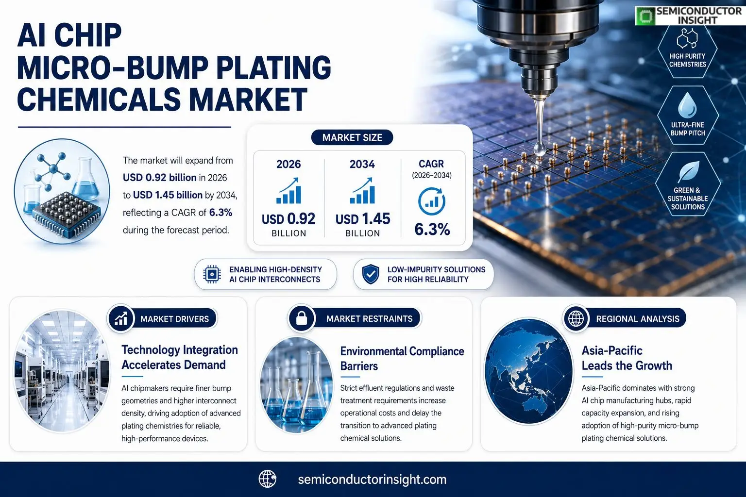
AI chip micro‑bump plating chemicals market size was USD 0.85 billion in 2025. The market will expand from USD 0.92 billion in 2026 to USD 1.45 billion by 2034, reflecting a CAGR of 6.3% during the forecast horizon.
Micro‑bump plating chemicals are specialized formulations used to deposit conductive metal layers on the tiny solder bumps that connect AI processors to substrates. These chemicals typically contain palladium‑based electroless solutions, copper seed layers, and organic additives that control surface tension and grain structure, enabling reliable electrical performance at sub‑10 µm bump pitches.The sector gains momentum because AI accelerators require ever‑greater interconnect density, which pushes manufacturers toward finer bump geometries and more robust plating chemistries. At the same time, advances in wafer‑level packaging and the shift toward heterogeneous integration create a steady demand for high‑purity reagents. Companies such as BASF SE, DuPont de Nemours, and Sumitomo Chemistry have broadened their portfolios with low‑impurity formulations designed for next‑generation AI chips.Furthermore, stricter environmental regulations in Europe encourage suppliers to develop water‑based alternatives that reduce hazardous waste while maintaining performance standards.
MARKET DRIVERS
Technology Integration Accelerates Demand
The surge in AI‑enabled processors pushes semiconductor manufacturers to adopt finer pitch interconnects. Micro‑bump plating chemicals become essential because they enable the dense copper pillars required for high‑bandwidth memory stacks. Faster data‑center workloads and edge‑AI inference workloads create a direct incentive for fab lines to upgrade plating chemistries, thereby expanding AI Chip Micro‑Bump Plating Chemicals Market.
Regulatory Incentives Shape Production
Governments in key semiconductor hubs have introduced clean‑room emission caps and waste‑water treatment subsidies. These policies reward suppliers that deliver low‑toxicity plating compounds, nudging OEMs toward newer chemical blends. Compliance‑driven procurement therefore fuels a shift away from legacy solvents, reinforcing market momentum.
➤ “Adoption of ultra‑low‑contamination plating agents is now a decisive factor in winning fab contracts.”
Beyond compliance, the strategic partnership between AI chip designers and packaging specialists encourages co‑development of plating solutions that meet both performance and reliability targets. This collaborative ecosystem strengthens AI Chip Micro‑Bump Plating Chemicals Market by aligning product roadmaps across the value chain.
MARKET CHALLENGES
Supply Chain Volatility
Recent geopolitical shifts have exposed fragilities in the raw‑material pipeline for specialty acids and complexing agents. Fab operators report longer lead times for high‑purity reagents, forcing them to hold larger safety stocks. Inventory pressure raises operating costs and can delay new product launches, posing a tangible obstacle for market participants.
Other Challenges
Cost Sensitivity
The intensive capital outlay required for upgrading plating lines makes budget allocation a critical decision point. Even modest price increases in proprietary chemistries can tip the economics against adoption, especially for smaller foundries that lack scale economies.
MARKET RESTRAINTS
Environmental Compliance Barriers
Stringent effluent standards in regions such as Taiwan and Germany demand additional treatment infrastructure for plating by‑products. Installing advanced neutralization systems adds both capital and operational overhead, dissuading some manufacturers from transitioning to newer chemical formulations. Regulatory cost burdens therefore restrain broader market penetration.
MARKET OPPORTUNITIES
Advanced Formulations for 3‑nm Nodes
Emerging AI chips targeting sub‑3‑nanometer process nodes require plating chemicals that deliver superior uniformity and reduced defectivity. Companies that can engineer additives to stabilize ultra‑thin copper deposits stand to capture a premium segment of AI Chip Micro‑Bump Plating Chemicals Market. Performance‑driven differentiation offers a clear pathway to higher margins.
AI Chip Micro-Bump Plating Chemicals Market Trends
Increasing Demand for Ultra‑Fine Bump Geometries
The transition of AI processors from discrete packages to wafer‑level integration has forced interconnect engineers to shrink solder bump dimensions below ten micrometres. This compression amplifies the role of plating chemistry because each micron of excess material can induce electrical resistance or mechanical stress. Suppliers are therefore refining palladium‑based electroless baths and copper seed layers to achieve uniform deposition across densely packed arrays. The result is a noticeable shift toward high‑purity, low‑particle formulations that can sustain consistent grain growth without compromising the delicate surface tension required for sub‑10 µm pitches. For manufacturers, the benefit is two‑fold: yields improve and the need for costly rework diminishes, which strengthens the overall economics of AI chip production.
Other Trends
Environmental and Regulatory Pressures Driving Water‑Based Solutions
European directives on hazardous waste have accelerated the migration from traditional solvent‑heavy chemistries to water‑based alternatives. Companies such as BASF SE and Sumitomo Chemistry are allocating R&D resources to replace hazardous organics with biodegradable surfactants that still satisfy the stringent conductivity and adhesion specifications of AI chip interconnects. This regulatory wake‑up is not merely compliance‑driven; it also opens new supply‑chain opportunities for firms that can certify low‑impact reagents, allowing them to capture a niche among OEMs eager to bolster their sustainability credentials.
Competitive Landscape Shifts Toward Integrated Service Offerings
Beyond raw chemicals, market players are bundling formulation expertise with process‑control tooling and on‑site technical support. DuPont de Nemours, for instance, leverages its legacy in polymer additives to offer turnkey plating lines that integrate real‑time monitoring of bath chemistry. This approach reduces variability for chipmakers and accelerates time‑to‑volume for next‑generation AI devices. As rivals emulate this model, the differentiation axis moves from product price alone to the breadth of value‑added services, prompting smaller niche suppliers to either specialize in ultra‑high‑purity grades or form strategic alliances with equipment manufacturers.
COMPETITIVE LANDSCAPEKey Industry Players
Competitive Dynamics in AI Chip Micro‑Bump Plating Chemicals
The AI chip micro‑bump plating chemicals sector is anchored by a handful of multinational suppliers that command the bulk of revenue. BASF SE leverages its extensive petrochemical platform to produce ultra‑low‑impurity palladium‑based electroless solutions, positioning the firm as a de‑facto standard‑setter for 7‑nm and smaller node processes. DuPont de Nemours complements this offering with copper seed formulations that integrate proprietary organic additives, enabling tighter control of grain structure across sub‑10 µm bump pitches. Sumitomo Chemical’s recent launch of a water‑based plating line has attracted AI‑focused fabs in Japan and Europe, where regulatory pressure favours reduced hazardous waste. Tokyo Ohka Kogyo (TOK) and Atotech round out the top tier, each delivering highly customized kits that blend metal salts with surfactants designed for heterogeneous integration workflows. Collectively these players shape pricing, dictate specification baselines, and lock in long‑term service contracts that raise entry barriers for newcomers.Beyond the dominant group, a diverse set of niche innovators supplies specialty components that address emerging packaging challenges. JSR Corporation specializes in organic additives that modulate surface tension for ultra‑fine bump arrays, while Hitachi High‑Technologies provides precision‑grade copper nitrate precursors tailored for wafer‑level packaging. Merck KGaA and Heraeus focus on catalyst‑grade palladium powders that improve plating uniformity in high‑throughput lines. Lanxess and H.C. Starck (now part of AMG) deliver custom‑engineered chelating agents that extend bath life under aggressive thermal cycles. Cabot Corporation and Umicore contribute high‑purity carbon‑based stabilizers that mitigate particle contamination, and Momentive offers silica‑based fluid modifiers that enhance wetting on novel substrate materials. These firms, though smaller in turnover, are crucial for differentiation, and their innovations often become the foundation for the next generation of AI chip interconnects.
List of Key AI Chip Micro‑Bump Plating Chemicals Companies Profiled
- BASF SE
- DuPont de Nemours
- Sumitomo Chemical
- Tokyo Ohka Kogyo (TOK)
- Atotech
- JSR Corporation
- Hitachi High‑Technologies
- Merck KGaA
- Heraeus
- Lanxess
- H.C. Starck (AMG)
- Cabot Corporation
- Umicore
- Momentive
Segment Analysis:
| Segment Category | Sub-Segments | Key Insights |
| By Type |
|
Electroless palladium solutions are prized for their ability to create uniform plating layers essential for sub‑10 µm bump pitches. They enable low defect density in high‑frequency AI chips and integrate smoothly with subsequent copper seed processes, supporting the exacting reliability requirements of modern AI accelerators. |
| By Application |
|
High‑density AI accelerator packaging drives the need for finer bump geometries, compelling the adoption of advanced plating chemistries. These formulations support thermal and electrical reliability under intense compute loads and align with the industry’s shift toward wafer‑level integration strategies. |
| By End User |
|
Semiconductor foundries prioritize specialized plating chemicals to meet aggressive production cycles. They favor high‑purity reagents that minimize contamination risks, ensuring the yield and performance expectations of next‑generation AI chips while embedding plating steps within sophisticated advanced packaging lines. |
| By Chemistry Composition |
|
Low‑impurity formulations reduce particle contamination that can trigger electrical failures, while enhancing metal grain structure for consistent conductivity. These chemistries satisfy the stringent quality standards demanded by AI‑centric devices and enable dependable performance across complex interconnect architectures. |
| By Environmental Regulation |
|
Europe REACH compliance pushes suppliers toward water‑based plating baths that lower hazardous waste generation. It also encourages the development of greener additive chemistries that retain performance, shaping supply‑chain practices as manufacturers align with the most rigorous environmental expectations. |
Regional Analysis: AI Chip Micro-Bump Plating Chemicals Market
North America
The region’s strength lies not only in capital availability but also in a dense network of research universities that feed talent into specialty chemical firms. As AI workloads demand tighter integration densities, the need for precise micro‑bump deposition becomes a decisive factor in product differentiation. Players that can deliver ultra‑low defect rates while maintaining throughput are gaining preference among leading chip makers.
Customer expectations are shifting toward environmentally compliant processes; thus, firms that incorporate greener surfactants and reduced waste streams are seeing stronger long‑term contracts. Moreover, the consolidation of foundry services under a few large entities creates a bargaining environment where volume discounts are tied to chemical performance guarantees.
In this competitive landscape, strategic partnerships between plating‑chemical providers and equipment OEMs are emerging as a practical route to co‑develop applications that align with the evolving lithography roadmap. The outcome is a market segment that rewards innovation, reliability, and sustainability in equal measure.
Silicon Valley and Boston host clusters where startups experiment with novel plating chemistries that support sub‑10 nm bump dimensions. These hubs attract venture capital seeking to back solutions that can shave a few picometers off line width, a margin that translates into measurable performance gains for AI accelerators.
The EPA’s tightening of hazardous air pollutant thresholds has prompted manufacturers to reformulate solvents. Companies adopting compliant blends early are positioning themselves as preferred suppliers for fabs that must meet strict environmental audits.
The merger of several major foundries under single corporate umbrellas creates a purchasing power dynamic where bulk contracts are linked to performance‑linked service agreements, raising the bar for chemical reliability.
Academic programs in surface chemistry and nanofabrication are expanding, delivering a steady flow of specialists who can translate laboratory breakthroughs into scalable production processes for AI‑focused chipmakers.
Europe
European nations combine strong environmental standards with a tradition of precision engineering. German chemical firms, in particular, have refined copper‑based plating solutions that emphasize low defectivity, a trait prized by fabs transitioning to 3‑nm processes. Meanwhile, France and the United Kingdom focus on collaborative research consortia that bring together universities, equipment manufacturers, and specialty chemical producers to address trace‑metal contamination challenges. The region’s regulatory framework, which stresses circular‑economy principles, pushes suppliers toward recyclable chemistries and reduced solvent emissions. As AI hardware demand intensifies, European customers prefer partners that can demonstrate both technical excellence and compliance with stringent sustainability metrics.
Asia‑Pacific
The Asia‑Pacific market is driven by rapid capacity expansion in China, Taiwan, and South Korea. Foundries in this corridor operate at scale, creating a fertile ground for chemical vendors that can deliver cost‑effective, high‑volume plating formulations. Local governments support the sector through subsidies aimed at shortening the time‑to‑market for AI chip designs, encouraging joint development projects that align plating chemistry with emerging packaging technologies such as fan‑out wafer‑level packaging. Cultural emphasis on speed and price competitiveness leads vendors to focus on process simplicity, yet the pressure to meet rising performance specifications ensures that quality remains a decisive factor.
South America
South American interest in the AI chip supply chain is emerging, largely centered around Brazil’s semiconductor research initiatives. While the region lacks large‑scale fabs, it offers a growing pool of chemical engineers trained in surface science, making it an attractive outsourcing destination for pilot‑scale plating trials. Government incentives aimed at diversifying industrial capabilities are prompting local chemical manufacturers to explore niche formulations that cater to low‑volume, high‑mix production lines. The strategic implication for players is the opportunity to establish early footholds through technology transfer agreements and joint R&D ventures.
Middle East & Africa
Investment in semiconductor‑related infrastructure is accelerating in the United Arab Emirates and Saudi Arabia, propelled by diversification agendas that target high‑tech industries. Although the region’s chemical production capacity remains modest, partnerships with established North American and European firms are enabling the transfer of advanced plating technologies. The emerging market environment favors flexible supply arrangements, where chemical providers can offer tailored support services to nascent fabrication facilities. For multinational vendors, these collaborations represent a pathway to embed themselves in future supply chains as the Middle East & Africa transition from import‑reliant to partially self‑sufficient markets.
Report Scope
This market research report provides a comprehensive analysis of the AI Chip Micro-Bump Plating Chemicals Market , covering the forecast period 2026–2034. It offers detailed insights into market dynamics, technological advancements, competitive landscape, and key trends shaping the industry.
Key focus areas of the report include:
- Market Overview: The report begins with an overview outlining its current market scenario, key growth indicators, and industry transformation drivers. It discusses macroeconomic factors, demand–supply balance, regulatory landscape, and the strategic role of semiconductors in powering advancements across industries such as automotive, telecommunications, consumer electronics, and industrial automation.
- Market Size & Forecast: Historical data and future projections for revenue, unit shipments, and market value across major regions and segments.
- Segmentation Analysis: Detailed breakdown by product type, technology, application, and end-user industry to identify high-growth segments and investment opportunities.
- Regional Insights: Insights into market performance across North America, Europe, Asia-Pacific, Latin America, and the Middle East & Africa, including country-level analysis where relevant.
- Competitive Landscape: Profiles of leading market participants, including their product offerings, R&D focus, manufacturing capacity, pricing strategies, and recent developments such as mergers, acquisitions, and partnerships.
- Technology Trends & Innovation: Assessment of emerging technologies, integration of AI/IoT, semiconductor design trends, fabrication techniques, and evolving industry standards.
- Market Drivers & Restraints: Evaluation of factors driving market growth along with challenges, supply chain constraints, regulatory issues, and market-entry barriers.
- Stakeholder Insights: Insights for component suppliers, OEMs, system integrators, investors, and policymakers regarding the evolving ecosystem and strategic opportunities.
Primary and secondary research methods are employed, including interviews with industry experts, data from verified sources, and real-time market intelligence to ensure the accuracy and reliability of the insights presented.
FREQUENTLY ASKED QUESTIONS:
What is the current market size of AI Chip Micro-Bump Plating Chemicals Market?
-> AI Chip Micro‑Bump Plating Chemicals Market was valued at USD 850 million in 2025 and is expected to reach USD 1,450 million by 2034, reflecting a CAGR of 6.3% over the forecast horizon.
Which key companies operate in AI Chip Micro-Bump Plating Chemicals Market?
-> Key players include BASF SE, DuPont de Nemours, and Sumitomo Chemistry, among others.
What are the key growth drivers?
-> Key growth drivers include rising interconnect density requirements for AI accelerators, expansion of wafer‑level packaging, heterogeneous integration trends, and increasing demand for high‑purity reagents.
Which region dominates the market?
-> Europe remains a dominant market due to stringent environmental regulations driving water‑based formulation development, while Asia‑Pacific shows rapid adoption driven by AI chip manufacturing hubs.
What are the emerging trends?
-> Emerging trends include development of water‑based and low‑impurity plating chemistries, integration of ultra‑pure palladium‑based electroless solutions, and innovations supporting heterogeneous integration of AI chips.
Get Sample Report PDF for Exclusive Insights
Report Sample Includes
- Table of Contents
- List of Tables & Figures
- Charts, Research Methodology, and more...
 Download Sample Report PDF





