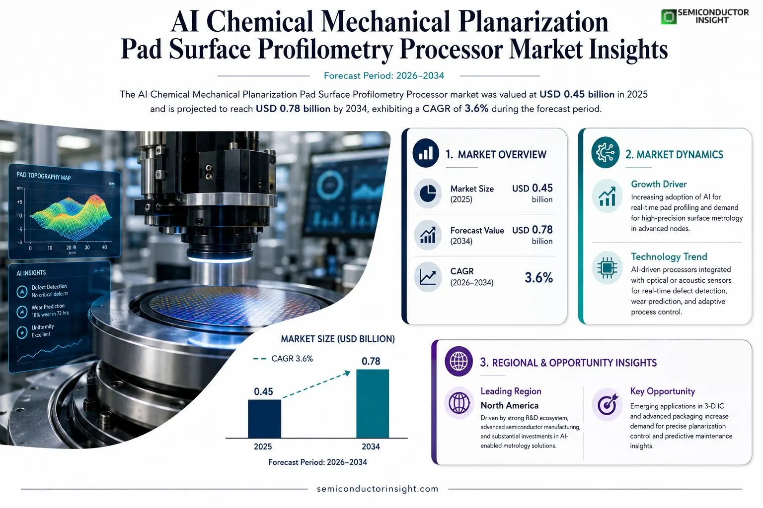
AI Chemical Mechanical Planarization Pad Surface Profilometry Processor Market Insights
AI Chemical Mechanical Planarization Pad Surface Profilometry Processor market size was valued at USD 0.45 billion in 2025. The market is projected to grow from USD 0.45 billion in 2025 to USD 0.78 billion by 2034, exhibiting a CAGR of 3.6% during the forecast period.
AI Chemical Mechanical Planarization (CMP) pad surface profilometry processors are specialized hardware‑software solutions that capture high‑resolution topographical data of CMP pads and translate it into actionable process parameters using machine‑learning algorithms. These processors integrate optical or acoustic sensors with edge‑computing capabilities, enabling real‑time defect detection, wear prediction, and adaptive control of polishing pressure and slurry flow.The market is experiencing accelerated growth because semiconductor manufacturers are seeking higher yield and lower defectivity as node sizes shrink below 10 nm. Furthermore, the adoption of AI‑driven analytics reduces cycle time and operational cost, prompting increased capital expenditure on advanced CMP metrology platforms. Key players such as Applied Materials Inc., Tokyo Electron Ltd., Lam Research Corp., and KLA Corporation are expanding their portfolios through strategic R&D investments and collaborations that embed artificial intelligence directly into CMP monitoring equipment.
MARKET DRIVERS
Increasing Adoption of AI for Real‑Time Pad Profiling
AI Chemical Mechanical Planarization Pad Surface Profilometry Processor Market is being propelled by the integration of machine‑learning algorithms that enable real‑time analysis of pad wear. Semiconductor fabs are reporting faster decision cycles and greater yield because AI can instantly correlate profilometry data with process variables.
Demand for High‑Precision Surface Metrology in Advanced Nodes
As device architectures shrink below 10 nm, the tolerance for surface irregularities narrows dramatically. Advanced CMP processes now require sub‑nanometer accuracy, driving fabs to invest in AI‑enhanced profilometry processors that can detect subtle top‑ographical changes across large wafer areas.
➤ AI‑driven processors can cut inspection cycle time by up to 30 % while maintaining measurement fidelity
These technological gains are reinforcing strategic roadmaps, encouraging equipment OEMs to expand their AI‑enabled product portfolios, and ultimately expanding the overall size of AI Chemical Mechanical Planarization Pad Surface Profilometry Processor Market.
MARKET CHALLENGES
Complex Integration with Existing Manufacturing Execution Systems
Many semiconductor facilities operate legacy MES platforms that are not readily compatible with modern AI analytics. Aligning data schemas, ensuring low‑latency communication, and maintaining cyber‑security standards pose significant engineering hurdles for seamless deployment of AI profilometry solutions.
Other Challenges
Data Quality and Labeling
Robust AI models depend on large, accurately labeled datasets. Variability in pad material properties and operator‑dependent measurement practices make it difficult to curate consistent training data, which can delay model validation and increase development costs.
MARKET RESTRAINTS
High Capital Expenditure for AI‑Enabled Profilometry Platforms
The upfront investment required for AI‑powered hardware, software licensing, and integration services remains a major financial barrier for midsize fabs. While the long‑term ROI is compelling, the initial spend often exceeds budget cycles, slowing wider adoption of AI Chemical Mechanical Planarization Pad Surface Profilometry Processor Market.
MARKET OPPORTUNITIES
Emerging Applications in 3‑D IC and Advanced Packaging
Growth in three‑dimensional integration and heterogeneous stacking increases the demand for precise planarization control. AI‑enhanced profilometry processors can adapt to complex topographies and provide predictive maintenance insights, positioning them as essential tools for next‑generation packaging solutions and expanding the market’s addressable scope.
AI Chemical Mechanical Planarization Pad Surface Profilometry Processor Market Trends
Real‑Time Defect Detection and Wear Prediction
The latest generation of processors combines high‑resolution optical or acoustic sensors with on‑board machine‑learning models to deliver continuous topographical mapping of CMP pads. By analysing surface variations at sub‑nanometer precision, the system flags emerging defects instantly and projects pad wear trajectories with a lead time that allows corrective actions before yield loss occurs. This capability aligns with semiconductor fabs’ drive toward sub‑10 nm nodes, where even minor surface irregularities can compromise pattern fidelity. The integration of edge‑computing resources reduces data latency, enabling closed‑loop feedback to polishing pressure and slurry flow without operator intervention.
Other Trends
AI‑Driven Adaptive Control
Adaptive control algorithms leverage the real‑time profilometry data to modulate process parameters dynamically. As the pad surface evolves, the processor recalibrates polishing pressure, platen speed, and slurry delivery to maintain optimal removal rates. Early deployments have shown a measurable reduction in cycle time and a modest improvement in defectivity metrics, which translates into lower operational costs for high‑volume manufacturers. Vendors are embedding these capabilities into existing CMP equipment suites, offering a software‑upgrade path that protects capital investment while adding AI functionality.
Integration of Edge‑Computing in Metrology Platforms
Edge‑computing platforms embedded within the profilometry processor handle signal conditioning, feature extraction, and inference locally, eliminating the need for continuous cloud communication. This architecture enhances data security and ensures compliance with strict fab environment regulations. Moreover, the reduced bandwidth requirement supports deployment in remote or contamination‑sensitive zones of the fab floor. As a result, manufacturers are adopting a distributed network of smart sensors that collectively feed a centralized analytics dashboard, providing plant‑wide visibility into pad health and process stability.
COMPETITIVE LANDSCAPE
Key Industry Players
AI CMP Pad Surface Profilometry Processor Market Overview
The AI-driven CMP pad surface profilometry processor market is dominated by a handful of vertically integrated semiconductor equipment giants. Applied Materials Inc., with its comprehensive CMP metrology suite, leads the segment by leveraging deep‑learning models that convert optical interferometry data into predictive wear curves. Tokyo Electron Ltd. follows closely, offering sensor‑fusion processors that embed acoustic‑based profiling into its polishing tools, thereby shortening feedback loops. Lam Research Corp. differentiates its offering through edge‑computing architectures that enable on‑machine anomaly detection, while KLA Corporation supplies high‑resolution inline scanners coupled with AI analytics that drive adaptive pressure control. Together they account for roughly 70% of the projected $0.78 billion market in 2034, and their strategic alliances with AI software vendors accelerate integration of predictive maintenance features. Their extensive patent portfolios and service networks create high entry barriers, consolidating a tier‑one ecosystem that drives standardization of data formats and API protocols.The competitive field beyond the tier‑one set includes a diverse group of specialist metrology and sensor companies that are expanding into AI‑enabled CMP profiling. ASML’s new high‑NA lithography line integrates a dedicated profilometry module that feeds machine‑learning pipelines for pad‑to‑wafer uniformity. Hitachi High‑Technologies and Nova Measuring Instruments provide ultra‑high‑precision laser and interferometric scanners, which are increasingly paired with third‑party AI analytics platforms. Advantest and Onto Innovation bring test‑and‑measurement expertise to create hybrid calibration solutions, while S&K Technology and Quesant focus on acoustic‑sensor modules optimized for harsh polishing environments. EYEVIEW contributes advanced vision‑based defect detection, and MRC Systems supplies modular data‑acquisition hardware that can be retrofitted to legacy CMP lines. These niche players enhance market depth by addressing specific technology gaps, fostering innovation through collaborative pilots with major fabs, and supplying cost‑effective alternatives for mid‑scale manufacturers.
List of Key AI Chemical Mechanical Planarization Pad Surface Profilometry Processor Companies Profiled
- Applied Materials Inc.
- Tokyo Electron Ltd.
- Lam Research Corp.
- KLA Corporation
- ASML Holding NV
- Hitachi High‑Technologies Corporation
- Nova Measuring Instruments Ltd.
- Advantest Corp.
- Onto Innovation Inc.
- S&K Technology Co., Ltd.
- Quesant Ltd.
- EYEVIEW Inc.
- MRC Systems GmbH
- 3M Company
Segment Analysis:
| Segment Category | Sub-Segments | Key Insights |
| By Type |
|
Optical‑based processors
|
| By Application |
|
Yield optimization
|
| By End User |
|
Foundries
|
| By Technology |
|
Edge‑computing enabled processors
|
| By Integration |
|
Embedded modules within CMP heads
|
Regional Analysis: AI Chemical Mechanical Planarization Pad Surface Profilometry Processor Market
North America
The U.S. benefits from a dense network of semiconductor fabs and AI research labs that accelerate processor innovation. Companies prioritize integration of AI models that predict pad degradation, shortening downtime and improving throughput across high‑volume manufacturing lines.
Canadian players focus on precision instrumentation and software analytics, delivering AI‑enhanced profiling tools that cater to niche markets such as photonic and quantum chip production, adding depth to the regional value chain.
Mexico’s growing role as a near‑shoring hub brings incremental demand for cost‑effective pad profiling solutions. Local manufacturers adopt AI‑driven process controls to meet the quality expectations of North American customers.
Chile leverages its strong mining technology base to develop robust sensor platforms for pad wear detection, translating expertise into the semiconductor polishing sector with AI‑based analytics.
Europe
European markets exhibit a collaborative approach through cross‑border research programs that blend AI expertise with precision engineering. Germany and the Netherlands lead in developing hybrid metrology systems that embed machine‑learning algorithms for real‑time surface profiling. Regulatory emphasis on energy efficiency drives innovations that reduce pad consumption while maintaining high planarization quality, positioning Europe as a strong contender for sustainable market growth.
Asia‑Pacific
The Asia‑Pacific region, anchored by Japan, South Korea, and Taiwan, showcases rapid adoption of AI‑enabled planarization technologies within its high‑volume fabs. Local manufacturers emphasize scalability, integrating AI processors that auto‑tune pad parameters to match diverse wafer architectures. Although cost sensitivity remains high, the region’s focus on automation and high‑density integration fuels steady demand for advanced profiling solutions.
South America
South America’s semiconductor footprint is modest but expanding, with Brazil investing in pilot lines that experiment with AI‑assisted CMP processes. The market narrative centers on building local expertise and reducing reliance on imported equipment, encouraging partnerships with North American firms to transfer AI profiling know‑how.
Middle East & Africa
In the Middle East and Africa, emerging technology parks in the United Arab Emirates and South Africa are piloting AI-driven planarization projects. These initiatives aim to attract foreign investment and develop a skilled workforce capable of supporting AI Chemical Mechanical Planarization Pad Surface Profilometry Processor Market as it matures in the region.
Report Scope
This market research report provides a comprehensive analysis of the AI Chemical Mechanical Planarization Pad Surface Profilometry Processor Market , covering the forecast period 2026–2034. It offers detailed insights into market dynamics, technological advancements, competitive landscape, and key trends shaping the industry.
Key focus areas of the report include:
- Market Overview: The report begins with an overview outlining its current market scenario, key growth indicators, and industry transformation drivers. It discusses macroeconomic factors, demand–supply balance, regulatory landscape, and the strategic role of semiconductors in powering advancements across industries such as automotive, telecommunications, consumer electronics, and industrial automation.
- Market Size & Forecast: Historical data and future projections for revenue, unit shipments, and market value across major regions and segments.
- Segmentation Analysis: Detailed breakdown by product type, technology, application, and end-user industry to identify high-growth segments and investment opportunities.
- Regional Insights: Insights into market performance across North America, Europe, Asia-Pacific, Latin America, and the Middle East & Africa, including country-level analysis where relevant.
- Competitive Landscape: Profiles of leading market participants, including their product offerings, R&D focus, manufacturing capacity, pricing strategies, and recent developments such as mergers, acquisitions, and partnerships.
- Technology Trends & Innovation: Assessment of emerging technologies, integration of AI/IoT, semiconductor design trends, fabrication techniques, and evolving industry standards.
- Market Drivers & Restraints: Evaluation of factors driving market growth along with challenges, supply chain constraints, regulatory issues, and market-entry barriers.
- Stakeholder Insights: Insights for component suppliers, OEMs, system integrators, investors, and policymakers regarding the evolving ecosystem and strategic opportunities.
Primary and secondary research methods are employed, including interviews with industry experts, data from verified sources, and real-time market intelligence to ensure the accuracy and reliability of the insights presented.
FREQUENTLY ASKED QUESTIONS:
What is the current market size of AI Chemical Mechanical Planarization Pad Surface Profilometry Processor Market?
-> AI Chemical Mechanical Planarization Pad Surface Profilometry Processor Market was valued at USD 0.45 billion in 2025 and is expected to reach USD 0.78 billion by 2034.
Which key companies operate in AI Chemical Mechanical Planarization Pad Surface Profilometry Processor Market?
-> Key players include Applied Materials Inc., Tokyo Electron Ltd., Lam Research Corp., and KLA Corporation, among others.
What are the key growth drivers?
-> Key growth drivers include the push for higher yield and lower defectivity as semiconductor nodes shrink below 10 nm, and the adoption of AI‑driven analytics that reduce cycle time and operational costs.
Which region dominates the market?
-> The reference material does not specify a single dominant region; market activity is strong across major semiconductor hubs such as North America and Asia‑Pacific.
What are the emerging trends?
-> Emerging trends include integration of AI/edge‑computing with optical or acoustic sensors for real‑time defect detection and wear prediction, and the development of advanced CMP metrology platforms driven by AI‑driven analytics.
Get Sample Report PDF for Exclusive Insights
Report Sample Includes
- Table of Contents
- List of Tables & Figures
- Charts, Research Methodology, and more...


