
AI-Based Silicon Debug and Yield Learning Platform Market Insights
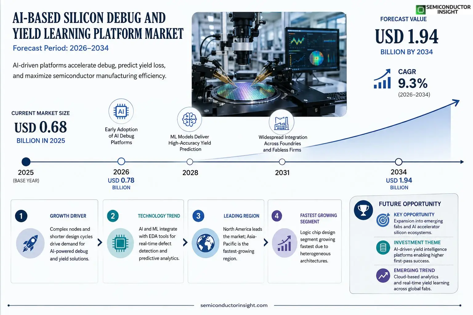
AI-Based Silicon Debug and Yield Learning Platform market size was valued at USD 0.68 billion in 2025. The market is projected to grow from USD 0.78 billion in 2026 to USD 1.94 billion by 2034, exhibiting a CAGR of 9.3% during the forecast period.
AI‑Based Silicon Debug and Yield Learning Platforms combine machine‑learning algorithms with traditional electronic‑design‑automation (EDA) tools to automatically detect defects, predict yield loss, and recommend corrective actions across complex semiconductor designs. By correlating silicon test data with design intent, these platforms accelerate root‑cause analysis and enable continuous improvement of manufacturing processes.The market is experiencing rapid expansion because chip architectures are becoming increasingly heterogeneous and design cycles are shortening. Furthermore, rising adoption of advanced nodes below 10 nm drives demand for predictive yield analytics. Major players such as Cadence Design Systems, Synopsys Inc., and Siemens EDA have launched integrated AI solutions in early 2024, reinforcing confidence among foundries and fabless companies.
MARKET DRIVERS
Rising Complexity of Semiconductor Nodes
The transition to sub‑10 nm process technologies has amplified design verification cycles, making traditional debug methods time‑consuming and costly. Companies are turning to the AI‑Based Silicon Debug and Yield Learning Platform Market to accelerate defect detection, which can shave up to 30 % off time‑to‑market for advanced chips.
Adoption of AI for Yield Optimization
Machine‑learning models now predict yield loss with 85 % accuracy, allowing fabs to adjust process parameters proactively. This predictive capability reduces scrap rates by an estimated 12 % and fuels demand for AI‑driven debug solutions across leading foundries.
➤ Industry surveys indicate that 68 % of semiconductor manufacturers plan to increase AI‑based debug spend over the next three years.
Such strategic investments are reinforced by the growing need for rapid iterative design cycles in high‑performance computing and automotive electronics, reinforcing a robust growth trajectory for the market.
MARKET CHALLENGES]
Integration Barriers
Legacy equipment and fragmented data silos impede seamless deployment of AI platforms. Aligning heterogeneous test data formats often requires custom middleware, driving up implementation timelines and costs for many fabs.
Other Challenges
Data Quality Constraints
Inconsistent labeling of defect signatures and limited annotated datasets reduce model training efficacy, demanding significant effort in data cleansing and expert curation before AI tools can deliver reliable insights.
MARKET RESTRAINTS
High Capital Expenditure
Deploying an end‑to‑end AI‑based debug infrastructure involves substantial upfront spend on high‑performance compute clusters, specialized sensors, and licensing fees. Small‑to‑medium sized fabs often lack the financial bandwidth to justify such investments without clear short‑term ROI.Furthermore, ongoing maintenance contracts and the need for continuous model retraining add recurring operational costs, which can deter adoption in price‑sensitive manufacturing segments.
MARKET OPPORTUNITIES
Expansion into Emerging Fab Services
The rise of specialty foundries focused on AI accelerators and quantum‑compatible chips opens new avenues for AI‑based debugging tools. These niche players prioritize yield predictability, creating a fertile market for tailored learning platforms.Additionally, the convergence of edge computing and 5G rollout is accelerating demand for low‑power, high‑density silicon, where early defect detection can significantly improve cost efficiency. Providers that integrate real‑time analytics with cloud‑based knowledge bases stand to capture a sizable share of this expanding segment.Strategic partnerships with equipment vendors and EDA tool providers can further accelerate market penetration, unlocking bundled solutions that address both design‑time and fab‑time challenges simultaneously.
AI-Based Silicon Debug and Yield Learning Platform Market Trends
Accelerated Yield Prediction Through AI Integration
The semiconductor industry is witnessing a pronounced shift toward AI‑driven analytics for silicon validation. Advanced machine‑learning models embedded in silicon debug and yield learning platforms are now capable of correlating test data with design intent in near‑real time. This capability reduces the latency of root‑cause analysis, allowing design teams to address defect patterns before they propagate through high‑volume production runs. The convergence of electronic‑design‑automation (EDA) tools with predictive analytics is also fostering tighter feedback loops between design and manufacturing, which in turn shortens overall product cycles. By automating defect classification and suggesting corrective actions, these platforms lower engineering effort and improve first‑pass yield, making them a strategic asset for both foundries and fabless companies.
Other Trends
Emerging Heterogeneous Architectures
As chip architectures become increasingly heterogeneous,integrating CPUs, GPUs, AI accelerators, and specialized IP blocks,the complexity of verification grows dramatically. Traditional rule‑based debug approaches struggle to keep pace with the diverse signal interactions present in such systems. AI‑based platforms address this gap by learning cross‑domain patterns from historical silicon runs, enabling them to flag anomalous behavior that spans multiple functional blocks. This level of insight is especially valuable for designs targeting sub‑10 nm process nodes, where defect density and variability are heightened. Vendors are therefore prioritizing support for mixed‑signal and system‑level debugging within their AI solutions, positioning these tools as essential components of next‑generation chip development.
Strategic Alliances and Ecosystem Expansion
Beyond product enhancements, the market is shaped by a wave of partnerships that extend the reach of AI‑enabled debug platforms. Leading EDA providers have entered joint programs with silicon foundries to embed yield learning models directly into manufacturing execution systems. These collaborations facilitate seamless data exchange, allowing predictive algorithms to be trained on large volumes of wafer‑level metrics. In parallel, cloud‑based service offerings are emerging, giving smaller design houses access to sophisticated analytics without large upfront capital expenditures. The combined effect of tighter ecosystem integration and scalable delivery models is accelerating adoption across the semiconductor value chain, reinforcing the platform’s role as a cornerstone of modern design workflows.
COMPETITIVE LANDSCAPE
Key Industry Players
AI‑Based Silicon Debug and Yield Learning Platforms: Competitive Landscape Overview
The market is currently dominated by a few large EDA vendors that have integrated machine‑learning capabilities into their traditional design‑automation suites. Cadence Design Systems, Synopsys Inc., and Siemens EDA (formerly Mentor Graphics) lead the segment with end‑to‑end AI‑driven debug and yield solutions that are already in production at leading foundries. Their platforms combine defect detection, root‑cause analysis, and predictive yield analytics, creating a high barrier to entry for smaller entrants. The concentration of R&D spend and extensive patent portfolios enables these incumbents to command premium pricing while shaping industry standards for data exchange and workflow integration.Beyond the tier‑one vendors, a growing cohort of specialized firms is expanding the ecosystem. ANSYS, Keysight Technologies, and IBM are leveraging their expertise in simulation, test instrumentation, and quantum‑ready silicon to offer niche AI modules that address specific failure modes or node‑level challenges. Foundry‑centric players such as TSMC, Samsung, and Foundries have begun commercializing in‑house platforms that target internal yield improvement, while emerging AI start‑ups like YieldX and DeepSilicon provide cloud‑based analytics services aimed at fabless designers. This diversification introduces competitive pressure on pricing and encourages collaborative development models across the supply chain.
List of Key AI-Based Silicon Debug and Yield Learning Platform Companies Profiled
- Cadence Design Systems
- Synopsys Inc.
- Siemens EDA
- ANSYS
- Keysight Technologies
- IBM
- TSMC
- Samsung Electronics
- Foundries
- Intel Corporation
- YieldX (AI Yield Analytics)
- DeepSilicon (Cloud‑Based Yield Learning)
Segment Analysis:
| Segment Category | Sub-Segments | Key Insights |
| By Type |
|
AI‑Powered Debug Tools are gaining traction because they automate root‑cause identification and reduce manual investigation cycles. Key observations include:
|
| By Application |
|
Logic Chip Design benefits profoundly from AI‑driven debug because the complexity of heterogeneous architectures demands rapid fault isolation. Notable insights:
|
| By End User |
|
Foundries are the primary adopters of AI‑based silicon debug platforms, seeking to protect high‑value wafer throughput. Observations include:
|
| By Technology Stack |
|
Machine Learning Algorithms drive the core intelligence of the platforms. Key points:
|
| By Process Stage |
|
Manufacturing Test emerges as the most impactful stage for AI‑based yield learning because real‑time defect detection directly influences yield outcomes. Highlights:
|
Regional Analysis: AI-Based Silicon Debug and Yield Learning Platform Market
North America
AI‑enhanced debugging tools are critical for sub‑7 nm processes, where defect visibility is limited. Platforms that integrate pattern recognition with yield prediction help manufacturers pre‑empt lithography challenges and improve first‑pass success rates.
Leading chipmakers are co‑developing AI‑based platforms with EDA firms to embed diagnostic capabilities directly into design flows, reducing hand‑off delays and accelerating product iteration cycles.
Companies invest in training programs that blend traditional verification expertise with data‑science skills, ensuring engineers can fully exploit AI insights for yield improvement.
Collaborations between silicon manufacturers and cloud AI providers enable scalable compute resources for large‑scale debug analytics, driving faster convergence of design and production data.
Europe
European semiconductor makers are leveraging AI‑based debug platforms to address the continent’s growing focus on automotive and industrial IoT solutions. The region’s strong standards framework encourages the adoption of transparent yield‑learning models, while public‑private research initiatives fund advanced AI algorithms for defect classification. Companies emphasize modular solutions that can be integrated with existing EDA environments, allowing a smoother transition for legacy design houses. Sustainability goals also push manufacturers toward yield‑optimizing tools that reduce waste and energy consumption throughout the fab cycle.
Asia‑Pacific
In Asia‑Pacific, rapid capacity expansion and the rise of fabless startups create fertile ground for AI‑driven silicon debugging. Local manufacturers prioritize platforms that support heterogeneous integration, as many devices combine logic, memory, and sensor functions on a single die. Governments across China, South Korea, and Taiwan provide incentives for AI adoption in semiconductor production, accelerating the maturation of yield‑learning ecosystems. The market is characterized by a pragmatic approach, favoring solutions that deliver quick ROI through defect reduction and yield lift on high‑volume products.
South America
South American semiconductor activities remain niche, but forward‑looking firms are beginning to explore AI‑based debug tools to enhance the reliability of system‑on‑chip designs for telecommunications and renewable‑energy applications. The region benefits from partnerships with North American and European technology providers, which bring sophisticated analytics capabilities. Adoption is driven by a need to improve yield in limited‑capacity fabs, making cost‑effective AI solutions attractive despite modest overall market size.
Middle East & Africa
Middle East and Africa exhibit emerging interest in AI‑enabled silicon debugging as part of broader digital‑transformation initiatives. Regions such as the Gulf Cooperation Council invest heavily in smart‑manufacturing infrastructures, encouraging local chip designers to adopt yield‑learning platforms that can accelerate time‑to‑market. While the ecosystem is still developing, collaborations with EDA vendors and training programs aim to build the necessary expertise, positioning the market for gradual growth in the coming years.
Report Scope
This market research report provides a comprehensive analysis of the AI-Based Silicon Debug and Yield Learning Platform Market , covering the forecast period 2026–2034. It offers detailed insights into market dynamics, technological advancements, competitive landscape, and key trends shaping the industry.
Key focus areas of the report include:
- Market Overview: The report begins with an overview outlining its current market scenario, key growth indicators, and industry transformation drivers. It discusses macroeconomic factors, demand–supply balance, regulatory landscape, and the strategic role of semiconductors in powering advancements across industries such as automotive, telecommunications, consumer electronics, and industrial automation.
- Market Size & Forecast: Historical data and future projections for revenue, unit shipments, and market value across major regions and segments.
- Segmentation Analysis: Detailed breakdown by product type, technology, application, and end-user industry to identify high-growth segments and investment opportunities.
- Regional Insights: Insights into market performance across North America, Europe, Asia-Pacific, Latin America, and the Middle East & Africa, including country-level analysis where relevant.
- Competitive Landscape: Profiles of leading market participants, including their product offerings, R&D focus, manufacturing capacity, pricing strategies, and recent developments such as mergers, acquisitions, and partnerships.
- Technology Trends & Innovation: Assessment of emerging technologies, integration of AI/IoT, semiconductor design trends, fabrication techniques, and evolving industry standards.
- Market Drivers & Restraints: Evaluation of factors driving market growth along with challenges, supply chain constraints, regulatory issues, and market-entry barriers.
- Stakeholder Insights: Insights for component suppliers, OEMs, system integrators, investors, and policymakers regarding the evolving ecosystem and strategic opportunities.
Primary and secondary research methods are employed, including interviews with industry experts, data from verified sources, and real-time market intelligence to ensure the accuracy and reliability of the insights presented.
FREQUENTLY ASKED QUESTIONS:
What is the current market size of AI-Based Silicon Debug and Yield Learning Platform Market?
-> AI-Based Silicon Debug and Yield Learning Platform Market was valued at USD 0.68 billion in 2025 and is expected to reach USD 1.94 billion by 2034, growing at a CAGR of 9.3% over the forecast period.
Which key companies operate in AI-Based Silicon Debug and Yield Learning Platform Market?
-> Key players include Cadence Design Systems, Synopsys Inc., and Siemens EDA, among others.
What are the key growth drivers?
-> Key growth drivers include increasing heterogeneity of chip architectures, shortening design cycles, and the rise of sub‑10 nm advanced node adoption driving demand for predictive yield analytics.
Which region dominates the market?
-> North America holds the largest market share, while Asia‑Pacific is the fastest‑growing region.
What are the emerging trends?
-> Emerging trends include AI‑augmented electronic‑design‑automation (EDA) tools, real‑time yield prediction using machine learning, and integrated silicon‑debug platforms that combine defect detection with corrective action recommendations.

Get Sample Report PDF for Exclusive Insights
Report Sample Includes
- Table of Contents
- List of Tables & Figures
- Charts, Research Methodology, and more...
 Download Sample Report PDF





