
AI-Based Overlay Control in Lithography Market Insights
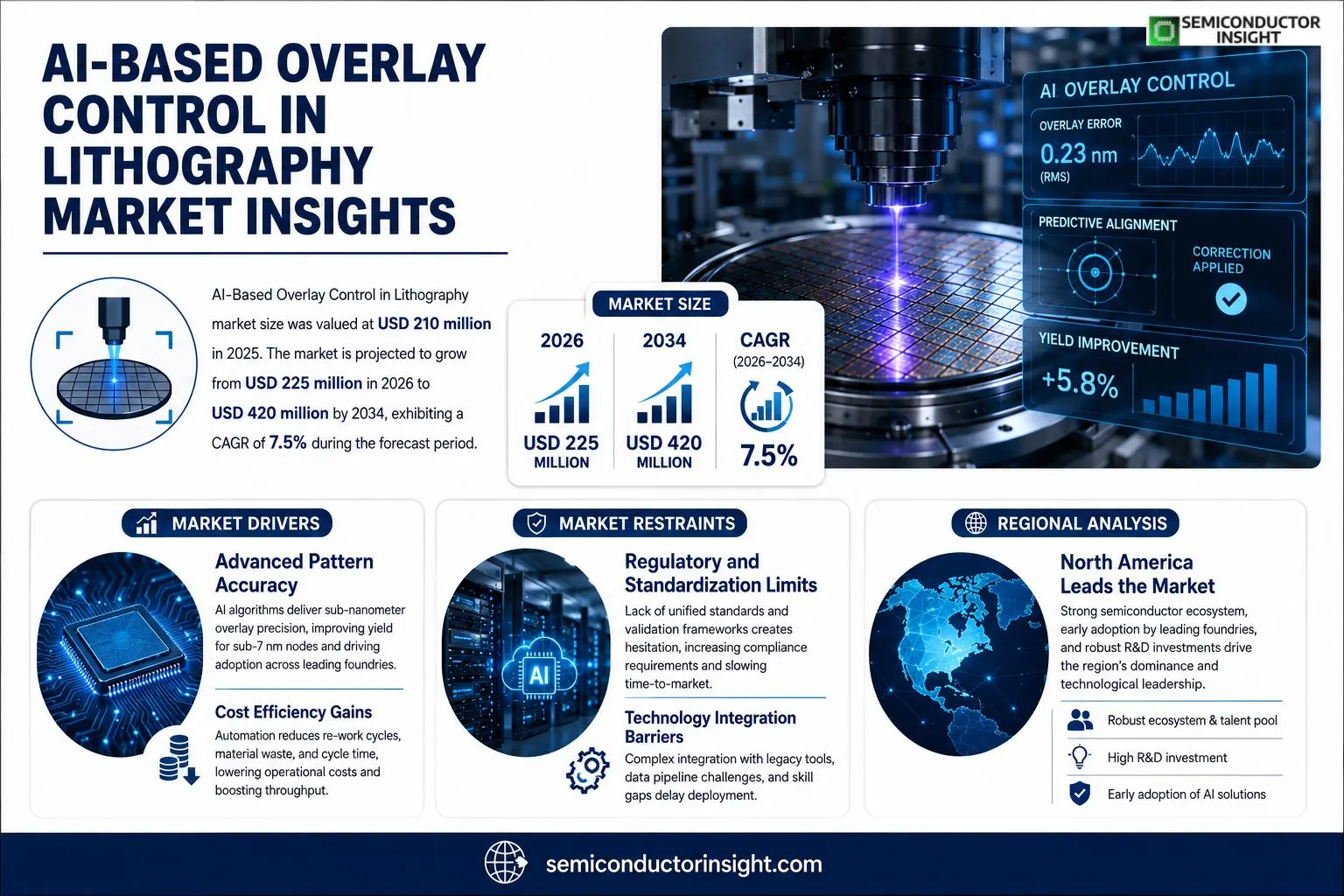
AI-Based Overlay Control in Lithography market size was valued at USD 210 million in 2025. The market is projected to grow from USD 225 million in 2026 to USD 420 million by 2034, exhibiting a CAGR of 7.5% during the forecast period.
AI‑Based Overlay Control refers to the application of machine‑learning algorithms and advanced image‑processing techniques to monitor and correct layer‑to‑layer alignment errors during semiconductor lithography. By analyzing sensor data from stepper/scanner tools in real time, these systems predict drift, compensate exposure variations, and reduce defectivity without manual intervention. The technology integrates deep‑neural networks with traditional overlay metrology, enabling sub‑nanometer precision that supports high‑NA EUV patterning and drives yield improvements across logic and memory fabs.
MARKET DRIVERS
Advanced Pattern Accuracy
AI-Based Overlay Control in Lithography Market is gaining traction because machine‑learning algorithms can predict and correct overlay errors in real time, delivering sub‑nanometer precision that traditional rule‑based systems cannot achieve. This heightened accuracy directly improves yield, especially for sub‑7 nm technologies, and is a primary catalyst for adoption across leading foundries.
Cost Efficiency Gains
By automating defect detection and reducing the number of re‑work cycles, AI solutions lower operational expenses and shorten cycle times. Manufacturers report a noticeable reduction in material waste and a smoother throughput, which translates into measurable cost savings for high‑volume production lines.
➤ “Deploying AI for overlay control has shifted our cost‑per‑wafer curve downwards while simultaneously boosting overall throughput.”
In addition, the scalability of cloud‑enabled AI platforms enables smaller fab operators to access sophisticated overlay control without massive capital outlays, further expanding the addressable market.
MARKET CHALLENGES
Technology Integration Barriers
Integrating AI models with legacy lithography equipment requires extensive calibration and data‑pipeline synchronization. Many plants face skill gaps in both semiconductor process engineering and data science, slowing the rollout of AI‑driven overlay solutions.
Other Challenges
Supply Chain Constraints
The specialized hardware (GPUs, high‑performance servers) needed for real‑time inference is subject to semiconductor shortages, which can delay implementation timelines.Furthermore, the need for continuous model retraining to accommodate new process recipes adds operational complexity and demands robust data governance frameworks.
MARKET RESTRAINTS
Regulatory and Standardization Limits
Absence of unified industry standards for AI validation in lithography creates hesitation among risk‑averse manufacturers. Compliance with existing quality‑assurance protocols often requires additional documentation and third‑party audits, which can increase time‑to‑market for new AI solutions.
MARKET OPPORTUNITIES
Emerging Applications in Advanced Nodes
The push toward 3‑nm and beyond opens a substantial opportunity for AI-Based Overlay Control in Lithography Market. As pattern densities increase, margin for error shrinks, making intelligent overlay correction indispensable. Early adopters that integrate AI now are positioned to capture premium market share as the technology matures.
AI-Based Overlay Control in Lithography Market Trends
Increasing Adoption of AI for Sub‑Nanometer Alignment
The semiconductor industry is accelerating its shift toward AI-driven overlay control as device geometries enter the sub‑10 nm regime. Machine‑learning models that analyze scanner sensor streams are now capable of detecting drift patterns that were previously invisible to conventional metrology. This capability reduces cycle‑time losses and improves yield consistency across logic and memory fabs. Early adopters report measurable reductions in defectivity, which translates into cost savings that justify the incremental investment in AI infrastructure. The trend is reinforced by the steady rollout of high‑NA extreme ultraviolet (EUV) scanners, whose tighter depth‑of‑focus budgets demand predictive alignment corrections in real time.
Other Trends
Integration with High‑NA EUV Tools
High‑NA EUV exposure tools generate larger diffraction‑limited spot sizes, increasing the sensitivity of overlay errors to thermal fluctuations. Vendors are embedding AI overlay control modules directly within the scanner control loop, allowing instantaneous compensation for temperature‑induced drift. This integration shortens the feedback loop from seconds to milliseconds, enabling patterning fidelity that meets the most aggressive design‑for‑manufacturing (DfM) specifications. Because the AI engine learns from each wafer, it continuously refines its prediction accuracy without manual re‑calibration.
Shift Toward Real‑Time Predictive Metrology
Traditional overlay metrology relies on post‑process measurements, creating a lag between error detection and correction. Real‑time predictive metrology leverages deep‑neural networks to forecast overlay deviations before they manifest on the wafer. By correlating sensor data from the stepper, wafer‑stage, and illumination system, the AI system predicts exposure‑induced shifts and proactively adjusts scanner parameters. This proactive approach not only improves process stability but also reduces the number of re‑work cycles, directly impacting fab throughput. Companies that have adopted predictive metrology report a 5‑10 % improvement in overall equipment effectiveness (OEE), underscoring the operational advantage of AI‑based overlay control.Overall, AI-Based Overlay Control in Lithography Market is moving from pilot projects to production‑level implementations. The convergence of advanced sensor suites, scalable cloud‑based training pipelines, and tighter design rules creates a fertile environment for continued innovation. As fabs pursue higher yields and lower defect levels, the strategic importance of AI overlay solutions will likely expand, positioning them as a core enabler of next‑generation semiconductor manufacturing.
COMPETITIVE LANDSCAPE
Key Industry Players
AI‑Based Overlay Control in Lithography – Competitive Overview
AI‑based overlay control market is anchored by a handful of equipment manufacturers that integrate advanced machine‑learning modules directly into stepper and scanner platforms. ASML Holding NV leads the segment, embedding predictive overlay algorithms in its NXT:2000i EUV systems and leveraging a robust service ecosystem to drive adoption across high‑volume fabs. This dominance creates a tiered structure where large‑scale lithography suppliers capture the majority of spend, while specialized metrology firms supply complementary sensors, calibration kits, and data‑analytics add‑ons. The market’s growth trajectory, underpinned by a 7.5 % CAGR through 2034, reinforces the strategic value of end‑to‑end solutions that combine hardware precision with AI‑driven feedback loops.Beyond the tier‑one leaders, a diverse set of niche players enriches the competitive landscape. KLA Corporation and Applied Materials offer dedicated overlay metrology suites that feed real‑time data to AI engines, while Tokyo Electron and Nikon provide cost‑effective scanners equipped with legacy overlay control features. Companies such as SUSS MicroTec and Bruker focus on high‑resolution inspection tools that enhance model training. EDA specialists including Synopsys and Cadence contribute algorithmic libraries for defect prediction, and semiconductor giants Intel, Samsung Electronics, and TSMC develop in‑house AI overlay solutions to protect proprietary process nodes. This ecosystem of specialized providers ensures innovation pressure across the value chain and creates opportunities for collaborative development.
List of Key AI‑Based Overlay Control Companies Profiled
- ASML Holding NV
- KLA Corporation
- Applied Materials Inc.
- Tokyo Electron Ltd.
- Nikon Corporation
- Canon Tokki Corporation
- SUSS MicroTec AG
- Bruker Nano GmbH
- Synopsys, Inc.
- Cadence Design Systems, Inc.
- Intel Corporation
- Samsung Electronics Co., Ltd.
- TSMC (Taiwan Semiconductor Manufacturing Company)
Segment Analysis:
| Segment Category | Sub-Segments | Key Insights |
| By Type |
|
Data‑driven AI is emerging as the primary driver because it leverages large volumes of sensor data to continuously refine overlay predictions.
|
| By Application |
|
Overlay correction for EUV lithography holds strategic significance as EUV tools demand sub‑nanometer precision.
|
| By End User |
|
Logic chip fabs are adopting AI‑based overlay control to meet aggressive scaling targets.
|
| By Technology |
|
Deep neural networks dominate because they efficiently capture complex, non‑linear overlay dynamics.
|
| By Process Stage |
|
In‑process drift compensation is gaining traction as it directly mitigates alignment errors while the wafer is still on the scanner.
|
Regional Analysis: AI-Based Overlay Control in Lithography Market
North America
Major North American foundries have incorporated AI‑based overlay control into high‑volume manufacturing, leveraging predictive analytics to anticipate alignment drift before it impacts yield. Early adoption provides a competitive edge, reinforcing the region’s leadership.
Government grants and private venture capital funnel billions into AI‑enhanced lithography research, fostering close collaboration between chipmakers and AI startups. This funding accelerates algorithm refinement and hardware integration.
A dense network of semiconductor OEMs, equipment manufacturers, and software vendors creates a virtuous cycle of feedback and improvement, ensuring that AI solutions remain tightly aligned with production needs.
Regional standards bodies actively endorse AI‑driven overlay metrics, enabling smoother compliance pathways and encouraging broader acceptance across the supply chain.
Europe
Europe maintains a strong position in AI-Based Overlay Control in Lithography Market through a combination of mature fabs and a vibrant ecosystem of research institutions. German and Dutch manufacturers are piloting AI overlay tools that integrate with existing EUV platforms, emphasizing sustainability and energy efficiency. Collaborative initiatives such as the European Chip Alliance foster knowledge exchange, while policy incentives aim to reduce the technology gap with North America. Nevertheless, adoption rates are moderated by cautious capital allocation and a fragmented market structure, resulting in a measured yet steady growth trajectory.
Asia‑Pacific
The Asia‑Pacific region, led by Taiwan, South Korea, and Japan, is rapidly scaling its AI overlay capabilities to meet surging demand for advanced nodes. Local chipmakers are leveraging close partnerships with AI startups to embed real‑time correction algorithms into high‑throughput lines. While cost‑sensitive scaling drives aggressive deployment, variations in regulatory frameworks and talent availability create uneven maturity across the sub‑regions. Overall, the region is poised to become a significant growth engine as AI integration matures.
South America
South America’s involvement in AI-Based Overlay Control in Lithography Market remains exploratory, with a focus on pilot projects in Brazil’s emerging semiconductor hubs. Academic collaborations are generating proof‑of‑concept models that aim to improve overlay precision for niche applications. Limited domestic production capacity and reliance on imported equipment constrain rapid expansion, but growing interest from multinational investors suggests a gradual buildup of capabilities.
Middle East & Africa
Middle East & Africa exhibits nascent activity in AI‑driven overlay control, primarily driven by government‑funded research centers in the United Arab Emirates and South Africa. These initiatives explore the integration of machine‑learning diagnostics into existing lithography equipment to enhance yield in specialized markets such as aerospace and defense. Infrastructure challenges and modest fab presence limit immediate market impact, yet strategic partnerships with vendors hint at future participation as regional expertise deepens.
Report Scope
This market research report provides a comprehensive analysis of the AI-Based Overlay Control in Lithography Market , covering the forecast period 2026–2034. It offers detailed insights into market dynamics, technological advancements, competitive landscape, and key trends shaping the industry.
Key focus areas of the report include:
- Market Overview: The report begins with an overview outlining its current market scenario, key growth indicators, and industry transformation drivers. It discusses macroeconomic factors, demand–supply balance, regulatory landscape, and the strategic role of semiconductors in powering advancements across industries such as automotive, telecommunications, consumer electronics, and industrial automation.
- Market Size & Forecast: Historical data and future projections for revenue, unit shipments, and market value across major regions and segments.
- Segmentation Analysis: Detailed breakdown by product type, technology, application, and end-user industry to identify high-growth segments and investment opportunities.
- Regional Insights: Insights into market performance across North America, Europe, Asia-Pacific, Latin America, and the Middle East & Africa, including country-level analysis where relevant.
- Competitive Landscape: Profiles of leading market participants, including their product offerings, R&D focus, manufacturing capacity, pricing strategies, and recent developments such as mergers, acquisitions, and partnerships.
- Technology Trends & Innovation: Assessment of emerging technologies, integration of AI/IoT, semiconductor design trends, fabrication techniques, and evolving industry standards.
- Market Drivers & Restraints: Evaluation of factors driving market growth along with challenges, supply chain constraints, regulatory issues, and market-entry barriers.
- Stakeholder Insights: Insights for component suppliers, OEMs, system integrators, investors, and policymakers regarding the evolving ecosystem and strategic opportunities.
Primary and secondary research methods are employed, including interviews with industry experts, data from verified sources, and real-time market intelligence to ensure the accuracy and reliability of the insights presented.
FREQUENTLY ASKED QUESTIONS:
What is the current market size of AI-Based Overlay Control in Lithography Market?
-> AI-Based Overlay Control in Lithography Market was valued at USD 210 million in 2025 and is expected to reach USD 420 million by 2034.
Which key companies operate in AI-Based Overlay Control in Lithography Market?
-> Key players include Axalta Coating Systems, AkzoNobel, BASF SE, PPG, Sherwin-Williams, and 3M, among others.
What are the key growth drivers?
-> Key growth drivers include railway infrastructure investments, urbanization, and demand for durable coatings.
Which region dominates the market?
-> Asia-Pacific is the fastest‑growing region, while Europe remains a dominant market.
What are the emerging trends?
-> Emerging trends include bio‑based coatings, smart coatings, and sustainable rail solutions.

Get Sample Report PDF for Exclusive Insights
Report Sample Includes
- Table of Contents
- List of Tables & Figures
- Charts, Research Methodology, and more...
 Download Sample Report PDF






