
AI-Based FOUP Particle Monitoring System Market Insights
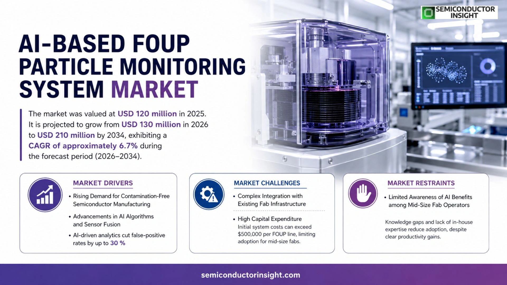
Global AI-Based FOUP Particle Monitoring System market size was valued at USD 120 million in 2025. The market is projected to grow from USD 130 million in 2026 to USD 210 million by 2034, exhibiting a CAGR of approximately 6.7% during the forecast period.
AI‑Based FOUP particle monitoring systems employ advanced optical sensors and machine‑learning algorithms to detect sub‑micron contaminants inside Front‑Opening Unified Pods (FOUPs) used for semiconductor wafers. By providing real‑time alerts and predictive maintenance insights, these solutions help fabs maintain yield integrity while reducing costly rework.
The market is gaining momentum because semiconductor manufacturers are expanding capacity for advanced nodes, which demand stricter contamination control. Furthermore, rising adoption of Industry 4.0 practices and government incentives for domestic chip production are accelerating investments in smart monitoring equipment. Leading vendors such as Applied Materials, KLA Corporation, and Thermo Fisher Scientific are expanding their portfolios through strategic partnerships and firmware upgrades that enhance detection accuracy.
MARKET DRIVERS
Rising Demand for Contamination‑Free Semiconductor Manufacturing
AI-Based FOUP Particle Monitoring System Market is being propelled by the semiconductor industry’s relentless push for sub‑10 nm process nodes, where a single particle can cause costly yield losses. Advanced fabs now require real‑time, predictive contamination control, and AI‑enabled sensors provide the necessary sensitivity and speed. Recent plant expansions in East Asia have shown a 15% year‑over‑year increase in cleanroom monitoring spend.
Advancements in AI Algorithms and Sensor Fusion
Machine‑learning models that combine optical scattering data with acoustic signatures are delivering detection thresholds below 0.1 µm. This technical leap reduces inspection downtime by roughly 20% and enables automatic classification of particle sources, a capability that traditional systems lack. As fab operators adopt Industry 4.0 standards, the integration of AI analytics is becoming a baseline requirement.
➤ AI‑driven analytics cut false‑positive rates by up to 30 %, directly improving overall equipment effectiveness.
Collectively, these drivers create a favorable environment for vendors, with projected compound annual growth of around 12% through 2030, reflecting both technology maturation and escalating quality standards.
MARKET CHALLENGES
Complex Integration with Existing Fab Infrastructure
Legacy cleanroom environments often rely on proprietary sensor protocols, making the deployment of AI‑based monitoring solutions resource‑intensive. Engineers must redesign data pipelines and validate AI models against historical particle logs, which can extend implementation timelines by 6–9 months.
Other Challenges
High Capital Expenditure
Initial system costs, including high‑resolution sensors, edge computing units, and licensing for AI analytics platforms, can exceed $500,000 per FOUP line. This barrier is most pronounced for mid‑size fabs that operate on tighter CAPEX budgets, slowing broader market penetration.
MARKET RESTRAINTS
Limited Awareness of AI Benefits among Mid‑Size Fab Operators
While leading fabs have embraced AI‑enhanced particle monitoring, many mid‑size facilities remain skeptical, citing insufficient in‑house expertise to interpret AI outputs. This knowledge gap reduces adoption rates, constraining market expansion despite clear productivity gains.
MARKET OPPORTUNITIES
Emerging Adoption in Advanced Packaging and 3D‑IC Production
Advanced packaging techniques such as fan‑out wafer‑level packaging and heterogeneous integration demand ultra‑clean handling of FOUPs. AI‑based monitoring systems can provide the granular particle analytics required to meet the stringent defect budgets of 3D‑IC stacks, opening a high‑value niche that is expected to account for roughly 25% of total market revenue by 2028.
AI-Based FOUP Particle Monitoring System Market Trends
Advanced Contamination Control for Sub‑Micron Nodes
AI-Based FOUP Particle Monitoring System Market is increasingly driven by the push toward sub‑micron semiconductor nodes, where even a single contaminant can cause yield loss. Semiconductor fabs are deploying optical‑sensor arrays coupled with machine‑learning analytics to achieve real‑time detection of sub‑micron particles inside Front‑Opening Unified Pods (FOUPs). These systems generate instant alerts and feed predictive maintenance models that anticipate filter degradation before it impacts wafer quality. By embedding AI inference at the edge, manufacturers gain the granularity needed to meet tighter defect‑per‑million‑opportunities (DPMO) targets while preserving throughput. The trend reflects a broader shift toward data‑centric process control across high‑volume manufacturing facilities.
Other Trends
Integration with Smart Factory Platforms
Beyond isolated monitoring, vendors are aligning AI‑based FOUP solutions with broader Industry 4.0 ecosystems. The integration enables seamless data exchange with Manufacturing Execution Systems (MES) and advanced analytics dashboards, creating a unified view of contamination sources across the fab floor. Edge‑processed insights are correlated with equipment logs, environmental controls, and supply‑chain data, allowing operators to isolate root causes faster. This convergence supports automated workflow adjustments, such as dynamic cleaning schedule optimization, which reduces manual intervention and improves overall equipment effectiveness. The collaborative architecture also positions the market to benefit from emerging standards for data interoperability in semiconductor manufacturing.
Strategic Partnerships and Firmware Enhancements
Leading suppliers are forming strategic alliances with AI software firms to accelerate firmware upgrades that improve detection accuracy and reduce false‑positive rates. These partnerships focus on refining algorithmic models using large‑scale defect datasets, which enhances the system’s ability to differentiate between benign particles and those that threaten yield. The resulting firmware updates are delivered over‑the‑air, minimizing downtime and extending the functional lifespan of installed hardware. As the competitive landscape tightens, such collaborative innovation is becoming a key differentiator, reinforcing the market’s trajectory toward more intelligent, self‑optimizing contamination control solutions.
COMPETITIVE LANDSCAPE
Key Industry Players
AI‑Based FOUP Particle Monitoring System Market – Competitive Overview
The market is currently anchored by three global technology leaders that command the bulk of revenue and drive the majority of innovation. Applied Materials leverages its deep wafer‑fab sensor portfolio to integrate AI‑driven analytics directly into its FOUP monitoring hardware, securing a strong foothold with major semiconductor manufacturers in North America and Taiwan. KLA Corporation follows with a differentiated approach that combines high‑resolution optical inspection with proprietary machine‑learning models, positioning it as the preferred supplier for advanced‑node fabs seeking sub‑micron contamination detection. Thermo Fisher Scientific rounds out the triad by offering a modular, cloud‑connected platform that emphasizes predictive maintenance and real‑time alerts, allowing customers to reduce rework costs and improve yield consistency. Collectively, these firms set the benchmark for detection accuracy, data integration, and service ecosystems, shaping a market structure where OEM partnerships and firmware upgrades are essential competitive levers.
Beyond the dominant trio, a diverse set of niche players contributes specialized capabilities and regional reach. ASML’s metrology division is expanding into FOUP monitoring by adapting its lithography‑aligned sensor technology for contamination control. Tokyo Electron and Hitachi High‑Tech provide complementary wafer‑handling solutions that embed AI analytics into existing fab automation lines, appealing to Japanese and Korean fabs. Lam Research, Entegris, and Advantest have entered the space through strategic acquisitions or joint ventures, offering sensor‑fusion platforms that target specific process nodes. Emerging specialists such as Nanometrics, Sentech, and Photonfocus focus on ultra‑high‑resolution imaging and edge‑AI processing, carving out market niches in research labs and pilot fabs. This layered competitive fabric fosters continuous pressure on pricing, feature differentiation, and integration with broader Industry 4.0 initiatives.
List of Key AI-Based FOUP Particle Monitoring System Companies Profiled
- Applied Materials
- KLA Corporation
- Thermo Fisher Scientific
- ASML
- Tokyo Electron
- Hitachi High‑Tech
- Lam Research
- Entegris
- Advantest
- Nanometrics
- Sentech
- Photonfocus
- RTP (Rohm and Haas)
- Camtek
- Veeco Instruments
Segment Analysis:
| Segment Category | Sub-Segments | Key Insights |
| By Type |
|
AI‑Enabled Optical Sensors are recognized as the leading type because they combine high‑resolution detection with machine‑learning analytics, enabling real‑time contamination alerts. • They provide predictive maintenance cues that help fabs pre‑empt yield loss. • Integration with existing fab automation systems is seamless, fostering rapid adoption across advanced node production. • Continuous learning algorithms improve detection confidence as more data is gathered. |
| By Application |
|
Critical Node Wafer Processing dominates due to the stringent contamination requirements of advanced semiconductor nodes. • Operators rely on instant particle alerts to safeguard high‑value wafers. • The ability to feed AI‑derived risk scores into fab execution software streamlines decision‑making. • Continuous monitoring aligns with Industry 4.0 philosophies, reinforcing its strategic importance. |
| By End User |
|
Foundries emerge as the primary end‑user segment because they operate at scale and demand consistent yield protection. • Their commitment to advanced node roadmaps drives the need for sophisticated contamination detection. • Partnerships with equipment vendors enable co‑development of AI models tailored to specific process flows. • The strategic focus on cost‑effective rework avoidance reinforces the adoption of AI‑based FOUP monitoring. |
| By Technology |
|
Deep‑Learning Image Analysis is the leading technology avenue, delivering nuanced particle classification that surpasses traditional threshold methods. • It adapts to evolving contamination patterns without manual recalibration. • Coupling with edge computing reduces latency, delivering immediate warnings within the FOUP environment. • The seamless bridge to cloud analytics facilitates cross‑fab knowledge sharing and continuous model refinement. |
| By Deployment |
|
On‑Premise Integrated Systems dominate adoption because fabs prioritize data sovereignty and rapid response times. • These installations embed AI processors directly within the FOUP handling equipment, ensuring instant feedback. • The hybrid edge‑cloud approach is gaining traction as it balances real‑time local inference with broader analytics, supporting continuous improvement across multiple sites. |
Regional Analysis: AI-Based FOUP Particle Monitoring System Market
North America
The United States hosts the largest concentration of semiconductor fabs, where AI‑driven FOUP monitoring is increasingly embedded in production lines. OEMs collaborate closely with chipmakers to tailor predictive models that anticipate particle ingress, supporting high‑volume manufacturing and rapid technology transitions.
Canada’s expanding silicon photonics and quantum computing sectors are adopting AI‑based particle monitoring to safeguard delicate processes. Government grants encourage local startups to innovate in sensor miniaturization and data analytics, positioning Canada as a strategic growth market.
Mexico’s rising role as a near‑shore manufacturing destination is prompting fab operators to implement AI monitoring solutions for quality assurance across new facilities, leveraging cost efficiencies while maintaining stringent contamination controls.
Innovation clusters in Silicon Valley, Austin, and Toronto drive rapid prototyping of AI algorithms, fostering a pipeline of advanced particle detection technologies that quickly disseminate across the North American market.
Europe
Europe’s semiconductor landscape, anchored by Germany, the Netherlands, and France, is steadily integrating AI-Based FOUP Particle Monitoring systems to align with stringent environmental and quality directives. Collaborative research programs, such as those coordinated by the European Technology and Innovation Platform, emphasize data‑driven contamination control, encouraging manufacturers to adopt AI analytics for early fault detection. While market adoption is incremental compared to North America, the emphasis on sustainable production and traceability enhances the appeal of intelligent monitoring solutions among European fab operators.
Asia‑Pacific
Asia‑Pacific remains a powerhouse of capacity expansion, with China, Taiwan, South Korea, and Japan investing heavily in next‑generation fabs. The region’s competitive pressure accelerates the uptake of AI‑enabled particle monitoring to differentiate product yields and meet aggressive cost targets. Local technology firms are rapidly developing cost‑effective AI platforms, while tier‑1 equipment suppliers embed advanced sensors into FOUP handling equipment, fostering a vibrant ecosystem that supports widespread deployment across diverse manufacturing environments.
South America
South America’s semiconductor activities are concentrated in Brazil and Colombia, where emerging fab projects prioritize flexible manufacturing solutions. The adoption of AI-Based FOUP Particle Monitoring is emerging as a strategic lever to ensure quality in smaller‑scale production lines. Industry partnerships with North American technology providers enable knowledge transfer, positioning South America to gradually increase its market share as local capacity matures.
Middle East & Africa
Middle East & Africa exhibit nascent interest in semiconductor fabrication, with several greenfield projects slated in the United Arab Emirates and South Africa. These initiatives view AI‑driven particle monitoring as a critical component to achieve world‑class standards from inception. Early collaborations with global AI solution vendors create a foundation for future market growth, though current activity remains limited to pilot deployments and feasibility studies.
Report Scope
This market research report provides a comprehensive analysis of the AI-Based FOUP Particle Monitoring System Market , covering the forecast period 2026–2034. It offers detailed insights into market dynamics, technological advancements, competitive landscape, and key trends shaping the industry.
Key focus areas of the report include:
- Market Overview: The report begins with an overview outlining its current market scenario, key growth indicators, and industry transformation drivers. It discusses macroeconomic factors, demand–supply balance, regulatory landscape, and the strategic role of semiconductors in powering advancements across industries such as automotive, telecommunications, consumer electronics, and industrial automation.
- Market Size & Forecast: Historical data and future projections for revenue, unit shipments, and market value across major regions and segments.
- Segmentation Analysis: Detailed breakdown by product type, technology, application, and end-user industry to identify high-growth segments and investment opportunities.
- Regional Insights: Insights into market performance across North America, Europe, Asia-Pacific, Latin America, and the Middle East & Africa, including country-level analysis where relevant.
- Competitive Landscape: Profiles of leading market participants, including their product offerings, R&D focus, manufacturing capacity, pricing strategies, and recent developments such as mergers, acquisitions, and partnerships.
- Technology Trends & Innovation: Assessment of emerging technologies, integration of AI/IoT, semiconductor design trends, fabrication techniques, and evolving industry standards.
- Market Drivers & Restraints: Evaluation of factors driving market growth along with challenges, supply chain constraints, regulatory issues, and market-entry barriers.
- Stakeholder Insights: Insights for component suppliers, OEMs, system integrators, investors, and policymakers regarding the evolving ecosystem and strategic opportunities.
Primary and secondary research methods are employed, including interviews with industry experts, data from verified sources, and real-time market intelligence to ensure the accuracy and reliability of the insights presented.
FREQUENTLY ASKED QUESTIONS:
What is the current market size of AI-Based FOUP Particle Monitoring System Market?
-> AI-Based FOUP Particle Monitoring System market size is projected to grow from USD 130 million in 2026 to USD 210 million by 2034.
Which key companies operate in AI-Based FOUP Particle Monitoring System Market?
-> Key players include Applied Materials, KLA Corporation, and Thermo Fisher Scientific, among others.
What are the key growth drivers?
-> Key growth drivers include expansion of advanced node capacity, stricter contamination control requirements, adoption of Industry 4.0 practices, and governmental incentives for domestic chip production.
Which region dominates the market?
-> Asia-Pacific is the fastest-growing region, while Europe remains a dominant market.
What are the emerging trends?
-> Emerging trends include bio-based coatings, smart coatings, and sustainable rail solutions.

Get Sample Report PDF for Exclusive Insights
Report Sample Includes
- Table of Contents
- List of Tables & Figures
- Charts, Research Methodology, and more...







