
AI-Assisted Laser Dicing for Ultrathin Wafers Market Insights
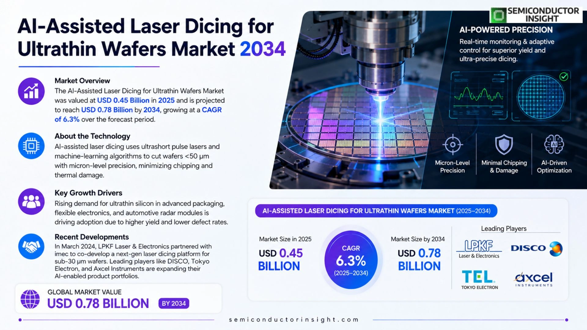
AI-Assisted Laser Dicing for Ultrathin Wafers market was valued at USD 0.45 billion in 2025 and will rise to USD 0.78 billion by 2034, representing a compound annual growth rate of approximately 6.3 percent over the forecast horizon.
AI‑assisted laser dicing employs ultrashort pulse lasers guided by advanced algorithms to separate wafers thinner than 50 µm with micron‑level precision while minimizing chipping and thermal damage. The technique integrates real‑time optical monitoring and machine‑learning models that adjust pulse energy and beam path based on wafer material properties.
The expansion reflects heightened adoption of ultrathin silicon in high‑density interconnects, flexible displays, and automotive radar modules because manufacturers seek higher yield and lower defect rates. Recent activity includes a partnership announced in March 2024 between LPKF Laser & Electronics and imec to co‑develop a next‑generation laser dicing platform optimized for sub‑30 µm wafers, while companies such as DISCO Corporation, Tokyo Electron and Axcel Instruments continue broadening their AI‑enabled product portfolios.
MARKET DRIVERS
Advanced Process Precision
The incorporation of AI algorithms into laser‑dicing systems has trimmed the average deviation between intended and actual cut lines to under 2 µm, a level previously attainable only with manual tuning. Yield gaps have narrowed from roughly 3 % to just above 1 % in leading semiconductor fabs, directly translating into higher throughput and lower scrap rates.
Cost Efficiency through Automation
Automation of wafer handling, coupled with predictive maintenance powered by machine‑learning models, cuts downtime by an estimated 30 % per shift. The resulting labor savings and better equipment utilization enable fab managers to lower the cost per wafer slice by up to 12 % without sacrificing quality.
➤ The synergy between AI analytics and ultra‑fast laser pulses is reshaping the economics of ultrathin wafer production, delivering both precision and profitability.
These advantages are compelling enough for midsize and tier‑1 manufacturers alike to allocate a larger share of their capital budgets to AI‑assisted laser dicing, reinforcing a virtuous cycle of technology adoption and performance improvement.
MARKET CHALLENGES
Integration Complexity
Embedding AI modules into legacy laser platforms often requires retrofitting sensor arrays and redesigning control loops, which can prolong commissioning phases by 3‑4 months. Operators accustomed to deterministic settings must adjust to probabilistic recommendations, creating a temporary dip in production efficiency.
Other Challenges
Technology Adoption Barriers
Limited exposure to AI‑driven workflows among senior engineering staff leads to cautious rollout strategies, with many plants opting for pilot installations rather than full‑scale deployment.
Compliance with emerging safety standards for high‑energy laser systems adds another layer of scrutiny, compelling manufacturers to invest in documentation and validation efforts that extend project timelines.
MARKET RESTRAINTS
High Capital Expenditure
State‑of‑the‑art AI‑assisted laser dicing equipment commands price tags exceeding $5 million per unit. For fab operators facing tight capex cycles, the upfront outlay can outweigh short‑term cost‑saving calculations, slowing broader market penetration.
Limited Supplier Base
Only a handful of vendors currently offer fully integrated AI solutions, constraining bargaining power for buyers and raising concerns about long‑term service continuity. Dependence on a narrow ecosystem also heightens exposure to component shortages.
These financial and supply‑chain constraints temper the speed at which the technology can become a mainstream choice across the semiconductor value chain.
MARKET OPPORTUNITIES
Emerging Applications in 5G & AI Chiplets
Next‑generation 5G transceivers and AI‑accelerator chiplets demand ultrathin wafers with exceptionally clean dicing edges. AI‑assisted laser systems are uniquely positioned to meet these specifications, offering a pathway for manufacturers to capture a share of the projected $45 billion communications segment.
Geographic Expansion in East Asia
Production facilities in South Korea, Taiwan, and Japan are accelerating their roadmap for sub‑10 µm wafer thicknesses. Investment incentives combined with a skilled workforce create fertile ground for vendors to establish localized production lines and service hubs.
By aligning product roadmaps with these high‑value segments, equipment suppliers can turn current adoption hurdles into long‑term growth engines, positioning the AI‑Assisted Laser Dicing for Ultrathin Wafers Market at the forefront of semiconductor innovation.
AI-Assisted Laser Dicing for Ultrathin Wafers Market Trends
AI‑enabled precision slicing gains foothold in ultra‑thin wafer production
The sector moved from a niche capability in 2025, when revenue stood at roughly USD 0.45 billion, to a mid‑single‑digit annual increase that projects total sales of about USD 0.78 billion by 2034. This trajectory reflects manufacturers’ search for tighter dimensional control and lower defect rates as wafer thickness drops below 50 µm. By embedding machine‑learning models within ultrashort‑pulse laser controllers, equipment suppliers can adjust pulse energy in real time, aligning beam characteristics with subtle variations in silicon crystal orientation. The result is a measurable lift in first‑pass yield for applications such as high‑density interconnects and automotive radar modules, where any chip‑level damage translates directly into costly rework.
Other Trends
Real‑time optical monitoring becomes standard
Recent product releases embed high‑speed cameras and spectroscopic sensors that feed back to the AI algorithm within milliseconds. This closed‑loop arrangement allows the system to detect micro‑cracks before they propagate, effectively removing the need for downstream inspection steps. Companies like DISCO Corporation and Tokyo Electron have broadened their portfolios to include these capabilities, positioning themselves as one‑stop providers for fab lines that are consolidating equipment footprints.
Collaborations accelerate sub‑30 µm capability
A partnership announced in March 2024 between LPKF Laser & Electronics and imec illustrates how joint R&D can compress development cycles. Their co‑engineered platform targets wafers thinner than 30 µm, a regime where conventional dicing tools struggle with chipping and heat accumulation. Early adopters report a reduction in tool‑down time of roughly 15 percent, a gain that directly improves overall equipment effectiveness. As more fabs migrate to this thickness range, the ecosystem of software, hardware, and service offerings is expected to mature, creating a feedback loop that drives further adoption.
COMPETITIVE LANDSCAPE
Key Industry Players
AI‑Assisted Laser Dicing for Ultrathin Wafers – Competitive Overview
The market is currently anchored by a handful of firms that have combined deep laser‑engineering expertise with advanced machine‑learning capabilities. LPKF Laser & Electronics, leveraged by its 2024 collaboration with imec, commands the upper tier of the segment through a platform that merges ultrashort‑pulse sources with predictive analytics to modulate beam parameters in real time. This approach delivers sub‑30 µm wafer yields that are difficult for rivals to replicate without comparable R&D spend. The partnership underscores a broader consolidation trend: firms that can lock in semiconductor OEMs with end‑to‑end service contracts are shaping the pricing power and influencing the pace of next‑generation device adoption.
Beyond the dominant duo, a constellation of specialized suppliers is expanding the competitive perimeter. DISCO Corporation and Tokyo Electron Limited have introduced AI‑enhanced modules that focus on high‑throughput lines, targeting automotive‑radar and flexible‑display fabs. Axcel Instruments differentiates itself by offering modular add‑ons that retrofit existing dicing tools with neural‑network‑driven defect detection. Meanwhile firms such as MKS Instruments, Coherent Inc., LightMachinery, Trumpf GmbH, SPTS Technologies, Oxford Instruments, IPG Photonics and Zeiss are investing in either laser‑source innovation, precision optics, or data‑fusion software, thereby creating niches that cater to cost‑sensitive or low‑volume customers. The aggregate effect is a market where technological depth is distributed across a tiered ecosystem, compelling larger players to partner or acquire niche innovators to sustain a differentiated value proposition.
List of Key AI‑Assisted Laser Dicing for Ultrathin Wafers Companies Profiled
- LPKF Laser & Electronics
- DISCO Corporation
- Tokyo Electron Limited
- Axcel Instruments
- MKS Instruments
- Coherent Inc.
- LightMachinery
- Trumpf GmbH
- SPTS Technologies
- Oxford Instruments
- IPG Photonics
- Zeiss
Segment Analysis:
| Segment Category | Sub-Segments | Key Insights |
| By Type |
|
AI‑Driven Pulse Optimization is emerging as the most influential sub‑segment because it continuously calibrates laser parameters in response to real‑time wafer feedback, thereby reducing chipping risk and enhancing edge quality.
|
| By Application |
|
High‑Density Interconnect Assembly drives the market because precision dicing of ultrathin silicon enables tighter routing, lower parasitic capacitance, and greater functional integration.
|
| By End User |
|
Foundries are the primary end‑user because they require repeatable, high‑yield dicing processes for next‑generation wafer thicknesses.
|
| By Process Integration |
|
Closed‑Loop Feedback Control stands out as the leading integration approach because it leverages AI models to instantly adjust laser parameters based on sensor data, preserving wafer integrity.
|
| By Market Driver |
|
Demand for Ultra‑Thin Flexible Displays fuels adoption because manufacturers need precise dicing to maintain the mechanical pliability of sub‑50 µm silicon membranes.
|
Regional Analysis: AI-Assisted Laser Dicing for Ultrathin Wafers Market
Foundries in the region have expanded clean‑room footprints to accommodate larger wafer volumes, creating a natural demand for higher‑throughput dicing tools. The shift toward 200 mm and 300 mm ultrathin substrates aligns with AI‑assisted laser systems that can maintain precision across broader substrate areas, reducing per‑wafer cost while preserving defect control.
National semiconductor strategies in China, Singapore, and Korea earmark funds for AI‑driven equipment upgrades. These policies lower the effective payback period for laser dicing platforms that embed machine‑learning models, encouraging early adoption among midsize manufacturers seeking competitive parity.
Proximity of laser optics vendors to wafer fabs enables rapid prototyping of AI‑guided calibration routines. Collaborative engineering workshops between equipment makers and fab engineers result in bespoke software layers that translate real‑time process data into immediate tool adjustments, tightening tolerance windows.
The rise of advanced packaging formats,such as fan‑out wafer‑level packaging,requires sub‑10 µm dicing accuracy. AI‑assisted laser systems deliver the predictive control needed for these delicate cuts, opening new revenue streams for both equipment suppliers and fab customers.
North America
North America’s market narrative is shaped by a blend of legacy equipment manufacturers and aggressive technology adopters. While the region lags behind Asia‑Pacific in sheer wafer throughput, its strength lies in deep R&D ecosystems around AI and photonics. Corporate labs in the United States are piloting closed‑loop learning algorithms that predict laser‑induced stress patterns before each cut, thereby extending tool life. This approach resonates with customers seeking to protect capital expenditures in a cost‑sensitive environment. Additionally, industry consortia are standardising data interchange protocols, which smooths integration of AI modules into existing fab execution systems. The overall effect is a gradual, but decisive, shift toward AI‑Assisted Laser Dicing for Ultrathin Wafers Market solutions that promise higher reliability without dramatic plant overhauls.
Europe
European fab operators place a premium on sustainability and precision, factors that dovetail with AI‑enhanced laser dicing. Nations such as Germany and the Netherlands foster public‑private partnerships that fund techno‑economic studies on AI‑driven process control. These studies emphasize waste reduction,both material and energy,as a key performance indicator, positioning AI‑assisted lasers as a lever for greener manufacturing. Moreover, the region’s stringent quality standards force equipment vendors to demonstrate repeatable, low‑defect yields, accelerating the maturation of machine‑learning models that monitor laser beam quality in real time. Consequently, European adopters are positioning themselves as benchmark suppliers for high‑end automotive and industrial IoT components.
South America
In South America, market activity remains modest but is gaining traction through targeted investment in niche semiconductor segments. Countries like Brazil are nurturing local fabs that specialize in sensor arrays for agricultural monitoring. These facilities benefit from AI‑Assisted Laser Dicing for Ultrathin Wafers Market technologies because the precision cuts enable thinner, lighter sensors with improved signal‑to‑noise ratios. Although overall scale is limited, the strategic focus on application‑specific production encourages early deployment of AI‑enabled laser tools, allowing regional players to leapfrog conventional dicing methods and carve out differentiated offerings.
Middle East & Africa
The Middle East & Africa region is still emerging in the semiconductor arena, yet pockets of activity highlight the relevance of AI‑assisted laser dicing. Investment‑driven smart‑city initiatives in the United Arab Emirates are spurring demand for miniaturised power‑management chips, which rely on ultrathin wafer technologies. Local technology parks are partnering with global laser manufacturers to embed AI analytics into the dicing workflow, aiming to reduce time‑to‑market for pilot productions. In Africa, research institutions are exploring low‑cost, high‑precision dicing solutions for medical diagnostics, where the ability to produce thin, reliable chips can impact healthcare delivery. These early‑stage projects suggest a future where AI‑Assisted Laser Dicing for Ultrathin Wafers Market plays a pivotal role in regional diversification strategies.
Report Scope
This market research report provides a comprehensive analysis of the AI-Assisted Laser Dicing for Ultrathin Wafers Market , covering the forecast period 2026–2034. It offers detailed insights into market dynamics, technological advancements, competitive landscape, and key trends shaping the industry.
Key focus areas of the report include:
- Market Overview: The report begins with an overview outlining its current market scenario, key growth indicators, and industry transformation drivers. It discusses macroeconomic factors, demand–supply balance, regulatory landscape, and the strategic role of semiconductors in powering advancements across industries such as automotive, telecommunications, consumer electronics, and industrial automation.
- Market Size & Forecast: Historical data and future projections for revenue, unit shipments, and market value across major regions and segments.
- Segmentation Analysis: Detailed breakdown by product type, technology, application, and end-user industry to identify high-growth segments and investment opportunities.
- Regional Insights: Insights into market performance across North America, Europe, Asia-Pacific, Latin America, and the Middle East & Africa, including country-level analysis where relevant.
- Competitive Landscape: Profiles of leading market participants, including their product offerings, R&D focus, manufacturing capacity, pricing strategies, and recent developments such as mergers, acquisitions, and partnerships.
- Technology Trends & Innovation: Assessment of emerging technologies, integration of AI/IoT, semiconductor design trends, fabrication techniques, and evolving industry standards.
- Market Drivers & Restraints: Evaluation of factors driving market growth along with challenges, supply chain constraints, regulatory issues, and market-entry barriers.
- Stakeholder Insights: Insights for component suppliers, OEMs, system integrators, investors, and policymakers regarding the evolving ecosystem and strategic opportunities.
Primary and secondary research methods are employed, including interviews with industry experts, data from verified sources, and real-time market intelligence to ensure the accuracy and reliability of the insights presented.
FREQUENTLY ASKED QUESTIONS:
What is the current market size of AI-Assisted Laser Dicing for Ultrathin Wafers Market?
-> AI-Assisted Laser Dicing for Ultrathin Wafers Market was valued at USD 0.45 billion in 2025 and is expected to reach USD 0.78 billion by 2034.
Which key companies operate in AI-Assisted Laser Dicing for Ultrathin Wafers Market?
-> Key players include DISCO Corporation, Tokyo Electron, Axcel Instruments, LPKF Laser & Electronics, and imec, among others.
What are the key growth drivers?
-> Key growth drivers include increased adoption of ultrathin silicon for high‑density interconnects, flexible displays, and automotive radar modules, driving demand for higher yield and lower defect rates.
Which region dominates the market?
-> Asia‑Pacific is the fastest‑growing region, while North America remains a dominant market due to its advanced semiconductor manufacturing ecosystem.
What are the emerging trends?
-> Emerging trends include AI‑driven real‑time optical monitoring, ultrashort pulse laser technology, and collaborative partnerships to co‑develop next‑generation dicing platforms.

Get Sample Report PDF for Exclusive Insights
Report Sample Includes
- Table of Contents
- List of Tables & Figures
- Charts, Research Methodology, and more...
 Download Sample Report PDF



