
Front-illuminated (FI) CMOS Sensor Market Insights
Front-illuminated (FI) CMOS Sensor market is projected to grow from USD 2,697 million in 2026 to USD 3,946 million by 2034, exhibiting a CAGR of 5.6% during the forecast period.
Front-illuminated (FI) CMOS Sensor, also known as Front‑side Illuminated (FSI) CMOS Sensor, is a classic image sensor that converts light into electrical signals for digital imaging. It employs a “top‑down” architecture where light passes through microlenses and color filters before reaching the metal wiring and circuit layer on the front side and finally the photodiodes – the photosensitive core. This foundational technology offers simple manufacturing, high yields and low cost, although the front metal layer blocks roughly 30% of incoming light, limiting utilization to about 70% and resulting in lower low‑light performance compared with back‑illuminated designs.
The demand for FI sensors stems from steady expansion of cost‑sensitive segments such as entry‑level consumer electronics, IoT devices and basic security monitoring, as well as consistent need for global shutter architectures in industrial automation and machine vision. Medical imaging adds incremental volume for certified units meeting clinical standards. Opportunities arise from refining process steps to boost quantum efficiency while preserving cost advantages, targeting emerging low‑power IoT and entry‑level automotive imaging markets, and delivering customized solutions for machine‑vision applications that prioritize global shutter performance over extreme low‑light capability.
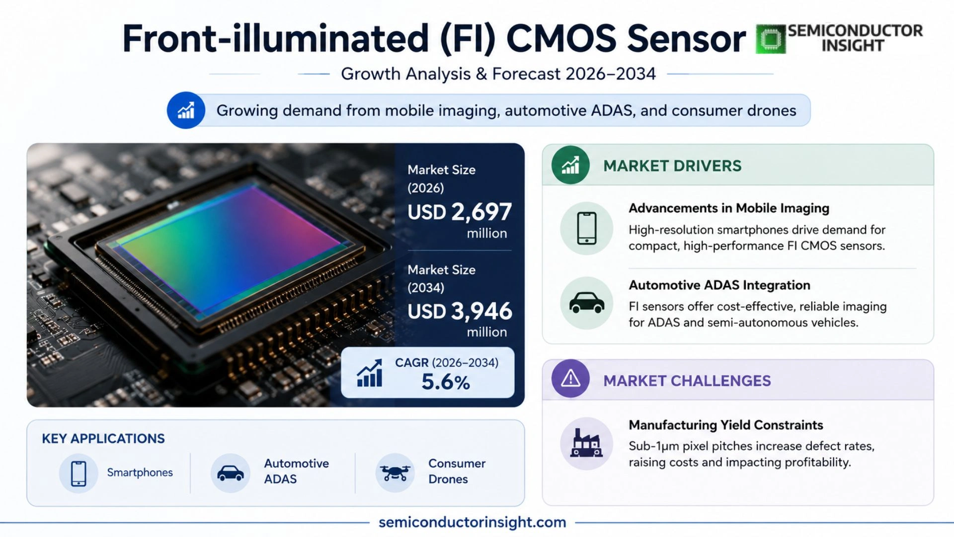
MARKET DRIVERS
Advancements in Mobile Imaging
The proliferation of high‑resolution photography in flagship smartphones has heightened the need for sensors that combine pixel density with strong low‑light response. Front-illuminated (FI) CMOS Sensor Market participants are capitalising on process refinements that shrink photodiode footprints while preserving quantum efficiency, enabling manufacturers to embed 50 MP modules without a proportional rise in device thickness.
Automotive ADAS Integration
Vehicle manufacturers are embedding camera‑based advanced driver‑assistance systems (ADAS) that rely on reliable, cost‑effective imaging components. FI sensors deliver the necessary field‑of‑view and durability for radar‑camera fusion, and their simpler stack architecture translates into lower bill‑of‑materials, a compelling advantage as OEMs scale production of semi‑autonomous platforms.
➤ Industry analysts note that the FI architecture’s reduced material stack shortens assembly cycle time, granting suppliers a competitive edge in price‑sensitive segments.
Beyond smartphones and cars, consumer‑grade drones are adopting FI sensors to meet budget constraints while still achieving acceptable video quality, signalling a broader market diffusion that bolsters overall growth prospects.
MARKET CHALLENGES
Manufacturing Yield Constraints
As pixel pitches shrink below 1 µm, defect density becomes a critical bottleneck. Foundries report that maintaining acceptable yield levels demands tighter process control, which inflates fab overhead and compresses margins for sensor makers targeting volume tiers.
Other Challenges
Supply Chain Volatility
Fluctuations in silicon wafer availability and the recent surge in semiconductor demand have introduced lead‑time uncertainty. Companies that cannot secure long‑term wafer contracts face schedule disruptions that reverberate throughout downstream device assemblers.
MARKET RESTRAINTS
Higher Power Consumption at Peak Performance
When FI sensors operate at their highest frame rates and resolutions, they tend to draw more current than their backside‑illuminated counterparts. This power draw necessitates larger battery packs or more aggressive thermal management, factors that deter integration in ultra‑thin devices.
Cost Competition from BSI Alternatives
Back‑side‑illuminated (BSI) sensors have narrowed the performance gap while offering superior light‑collection efficiency. Their gradual price decline erodes the traditional cost advantage of FI designs, compelling manufacturers to justify the selection on parameters other than price alone.
Regulatory Hurdles for Automotive Deployments
Automotive applications must satisfy stringent functional safety standards (ISO 26262). The certification process adds time and expense, and any deviation from established sensor architectures can trigger additional validation cycles, slowing market entry for new FI models.
MARKET OPPORTUNITIES
Emerging Wearable Applications
Wearable devices such as smart glasses and health‑monitoring bands are demanding compact imaging solutions that balance resolution with power efficiency. FI sensors, with their shallow stack and modest cost, align well with the ergonomic constraints of head‑mounted displays, opening a niche with limited competition.
IoT Edge Cameras
Edge‑computing cameras deployed in smart factories and retail analytics require on‑device processing and affordable optics. The FI sensor’s lower fabrication complexity enables manufacturers to embed AI accelerators alongside the sensor die, delivering intelligent vision at the edge without inflating unit cost.
Medical Imaging Miniaturisation
Portable diagnostic tools, including handheld endoscopes, benefit from the shallow form factor of FI sensors. Their ability to maintain adequate signal‑to‑noise ratios in constrained lighting environments positions them as viable components for next‑generation point‑of‑care imaging equipment.
Front-illuminated (FI) CMOS Sensor Market Trends
Cost‑Driven Adoption in Consumer and IoT Segments
Front-illuminated (FI) CMOS Sensor Market recorded revenues of roughly $2.7 billion in 2025 and is forecasted to reach about $3.9 billion by 2034. Production volumes topped 1.64 billion units that year, with an average transaction price near $1.80 per kilounit. These figures reflect the sensor’s enduring appeal where price sensitivity outweighs the need for extreme low‑light performance. Applications such as entry‑level smartphones, wearable gadgets, and connected home devices capitalize on the sensor’s straightforward manufacturing flow and high yield, keeping component costs low while delivering acceptable image quality for everyday use. The modest light‑utilization rate of roughly 70 %,a consequence of the front‑metal stack,remains acceptable in well‑lit environments, cementing the sensor’s position as the workhorse of cost‑conscious imaging solutions.
Other Trends
Industrial Automation and Global Shutter Preference
In manufacturing and machine‑vision contexts, the demand for global‑shutter enabled FI sensors has stayed resilient. Factories that rely on precise motion capture favor the read‑out architecture that eliminates rolling‑shutter distortion, even though the light‑sensitivity trade‑off is less critical than in consumer photography. The sensor’s ability to be produced at scale with minimal defect rates makes it a logical choice for robotics, quality‑control stations, and high‑throughput inspection lines. Moreover, the medical imaging niche,particularly devices requiring certified components,has introduced a modest yet steady stream of orders, reinforcing the sensor’s versatility across regulated environments.
Process Optimization as a Competitive Lever
Manufacturers are channeling R&D resources toward refining the front‑side architecture to squeeze additional photons from the same aperture. Techniques such as microlens redesign, thinner metal interconnects, and optimized color‑filter stacks are being trialed to lift effective quantum efficiency toward the mid‑70 % range without sacrificing the low‑cost advantage. Parallel efforts focus on noise‑reduction algorithms embedded in sensor firmware, enhancing signal‑to‑noise ratios for borderline lighting conditions. Companies that master these incremental gains can defend market share against back‑illuminated alternatives while opening doors to emerging low‑power IoT cameras and budget‑oriented automotive imaging modules, where price margins are razor‑thin but volume potential is massive.
COMPETITIVE LANDSCAPE
Key Industry Players
Competitive dynamics among leading FI CMOS sensor manufacturers
Sony dominates the front‑illuminated CMOS sensor arena, leveraging its deep photodiode expertise and scale‑driven cost efficiencies. The company’s ability to integrate global‑shutter architectures within a mature production line sustains its market share in both consumer‑grade and industrial segments. Sony’s extensive IP portfolio and its strategic focus on incremental light‑sensitivity improvements keep it ahead of cost‑sensitive rivals, allowing the firm to command premium pricing for higher‑resolution modules while still competing on volume. This concentration around a single powerhouse shapes pricing benchmarks and drives smaller players toward niche differentiation or regional specialization.
Beyond Sony, the competitive set fragments into a mix of diversified semiconductor giants and specialist firms. Samsung and OmniVision exploit advanced wafer‑fab capacity to supply mid‑tier FI sensors for entry‑level smartphones and IoT devices, emphasizing aggressive price points. STMicroelectronics and ON Semiconductor (Onsemi) concentrate on industrial automation, where global‑shutter performance outweighs low‑light sensitivity, delivering customized solutions for machine‑vision OEMs. SK Hynix and GalaxyCore have entered the market to capture emerging demand in cost‑constrained automotive imaging, while Panasonic and Canon apply their optical heritage to medical‑grade FI sensors that must meet stringent regulatory standards. Smaller innovators such as SmartSens Technology, Silicon Optronics, Sharp and Toshiba differentiate through ultra‑small pixel designs or multi‑spectral extensions, targeting emerging low‑power edge applications. The resulting ecosystem reflects a balance between scale advantages and targeted specialization, compelling incumbents to refine process yields while prompting newcomers to carve out narrowly defined value propositions.
List of Key Front-illuminated (FI) CMOS Sensor Companies Profiled
- Sony, Samsung, OmniVision, STMicroelectronics
- ON Semiconductor, SK Hynix, GalaxyCore, Panasonic
- SmartSens Technology, Canon, Silicon Optronics, Sharp, Toshiba
Segment Analysis:
| Segment Category | Sub-Segments | Key Insights |
| By Type |
|
Standard FI Sensor
|
| By Application |
|
Consumer Electronics
|
| By End User |
|
Cost‑Conscious Consumer Devices
|
| By Pixel Size |
|
Medium Pixel FI Sensors
|
| By Spectral Response |
|
Visible Light FI Sensors
|
Regional Analysis: Front-illuminated (FI) CMOS Sensor Market
Asia-Pacific
Recent expansions in 300‑mm fabs across Taiwan, South Korea and China have lifted output ceilings, enabling manufacturers to meet the surge in high‑resolution sensor orders. The shift toward wafer‑scale integration reduces per‑unit cost and improves consistency across product families, a critical factor for volume‑driven appliance makers.
Companies are diversifying raw material sources and bolstening logistics networks to mitigate geopolitical friction. Strategic stockpiling of silicon wafers and localized packaging facilities have shortened lead times, ensuring smoother fulfillment for automotive tier‑1 suppliers.
Mobile imaging remains the dominant driver, but the region is witnessing rapid adoption of FI sensors in autonomous‑driving camera stacks and industrial machine‑vision rigs. The convergence of miniaturization and low‑light performance requirements is widening the addressable market.
Harmonized environmental standards across ASEAN and Greater China facilitate cross‑border component flow. Meanwhile, relaxed export controls on photonic equipment have accelerated technology transfer, allowing smaller firms to scale more quickly.
North America
In North America, the market narrative is shaped by an emphasis on advanced driver‑assistance systems and high‑end consumer electronics. A handful of fabless innovators leverage deep R&D budgets to push pixel‑type innovations, while contract manufacturers in the United States focus on low‑defect assembly for premium devices. The region’s regulatory emphasis on data privacy has spurred demand for on‑sensor processing, nudging OEMs toward FI architectures that can embed preprocessing capabilities. Though domestic wafer capacity is limited compared with Asia, strategic partnerships with overseas foundries offset the shortfall and keep supply chains agile.
Europe
European activity centers on automotive safety and industrial automation, where stringent functional‑safety certifications drive sensor selection criteria. Companies based in Germany and France are pioneering sensor‑fusion algorithms that rely on FI devices for their superior quantum efficiency under limited illumination. Collaborative research programs funded by the EU encourage co‑development of heterogeneous integration techniques, merging sensors with AI accelerators on a single die. While volume manufacturing remains export‑oriented, the region’s design expertise continues to shape product roadmaps for global brands.
South America
South American markets exhibit a cautious but growing appetite for FI sensors, primarily in consumer electronics imports and localized medical imaging equipment. Brazil’s recent tax incentives for semiconductor assembly have attracted modest investment, allowing regional firms to assemble and test sensors for domestic distribution. The ecosystem is still dependent on imported wafers, but improved logistics corridors are reducing lead times. As smartphone penetration deepens, end‑users are demanding better low‑light performance, prompting importers to favor FI solutions over legacy options.
Middle East & Africa
The Middle East & Africa region is driven by surveillance and smart‑city initiatives that require reliable imaging under diverse lighting conditions. Investments in data‑center infrastructure have encouraged OEMs to adopt sensors with higher dynamic range, a niche where FI technology excels. In the United Arab Emirates, government‑backed pilots for autonomous public transport are evaluating sensor stacks that integrate FI chips for robust perception. Although local fabrication is minimal, the region’s role as a testing ground for high‑performance applications is expanding, creating downstream demand for specialized sensor modules.
Report Scope
This market research report provides a comprehensive analysis of the Front-illuminated (FI) CMOS Sensor Market , covering the forecast period 2026–2034. It offers detailed insights into market dynamics, technological advancements, competitive landscape, and key trends shaping the industry.
Key focus areas of the report include:
- Market Overview: The report begins with an overview outlining its current market scenario, key growth indicators, and industry transformation drivers. It discusses macroeconomic factors, demand–supply balance, regulatory landscape, and the strategic role of semiconductors in powering advancements across industries such as automotive, telecommunications, consumer electronics, and industrial automation.
- Market Size & Forecast: Historical data and future projections for revenue, unit shipments, and market value across major regions and segments.
- Segmentation Analysis: Detailed breakdown by product type, technology, application, and end-user industry to identify high-growth segments and investment opportunities.
- Regional Insights: Insights into market performance across North America, Europe, Asia-Pacific, Latin America, and the Middle East & Africa, including country-level analysis where relevant.
- Competitive Landscape: Profiles of leading market participants, including their product offerings, R&D focus, manufacturing capacity, pricing strategies, and recent developments such as mergers, acquisitions, and partnerships.
- Technology Trends & Innovation: Assessment of emerging technologies, integration of AI/IoT, semiconductor design trends, fabrication techniques, and evolving industry standards.
- Market Drivers & Restraints: Evaluation of factors driving market growth along with challenges, supply chain constraints, regulatory issues, and market-entry barriers.
- Stakeholder Insights: Insights for component suppliers, OEMs, system integrators, investors, and policymakers regarding the evolving ecosystem and strategic opportunities.
Primary and secondary research methods are employed, including interviews with industry experts, data from verified sources, and real-time market intelligence to ensure the accuracy and reliability of the insights presented.
FREQUENTLY ASKED QUESTIONS:
What is the current market size of Front-illuminated (FI) CMOS Sensor Market?
-> Global Front-illuminated (FI) CMOS Sensor market is projected to grow from USD 2,697 million in 2026 to USD 3,946 million by 2034, exhibiting a CAGR of 5.6%
Which key companies operate in Front-illuminated (FI) CMOS Sensor Market?
-> Key players include SONY, Samsung, OmniVision, STMicroelectronics, Onsemi, SK Hynix, GalaxyCore, Panasonic, SmartSens Technology, Canon, and Silicon Optronics, among others.
What are the key growth drivers?
-> Key growth drivers include steady demand from cost‑sensitive consumer electronics, expanding IoT device deployments, increasing security‑monitoring installations, rising adoption of global‑shutter architectures in industrial automation and machine vision, and incremental demand from medical imaging applications requiring certified FI sensors.
Which region dominates the market?
-> Asia‑Pacific holds the largest market share, driven by high manufacturing capacity and robust demand in consumer electronics and automotive sectors, while North America and Europe remain important secondary markets.
What are the emerging trends?
-> Emerging trends include integration of FI sensors with AI‑enabled edge processing, development of ultra‑low‑power designs for battery‑operated IoT devices, customization for entry‑level automotive imaging, and advances in global‑shutter technologies to improve motion‑capture performance in industrial machine‑vision systems.

Get Sample Report PDF for Exclusive Insights
Report Sample Includes
- Table of Contents
- List of Tables & Figures
- Charts, Research Methodology, and more...
 Download Sample Report PDF



