3D Stacked CMOS Image Sensor Market Insights
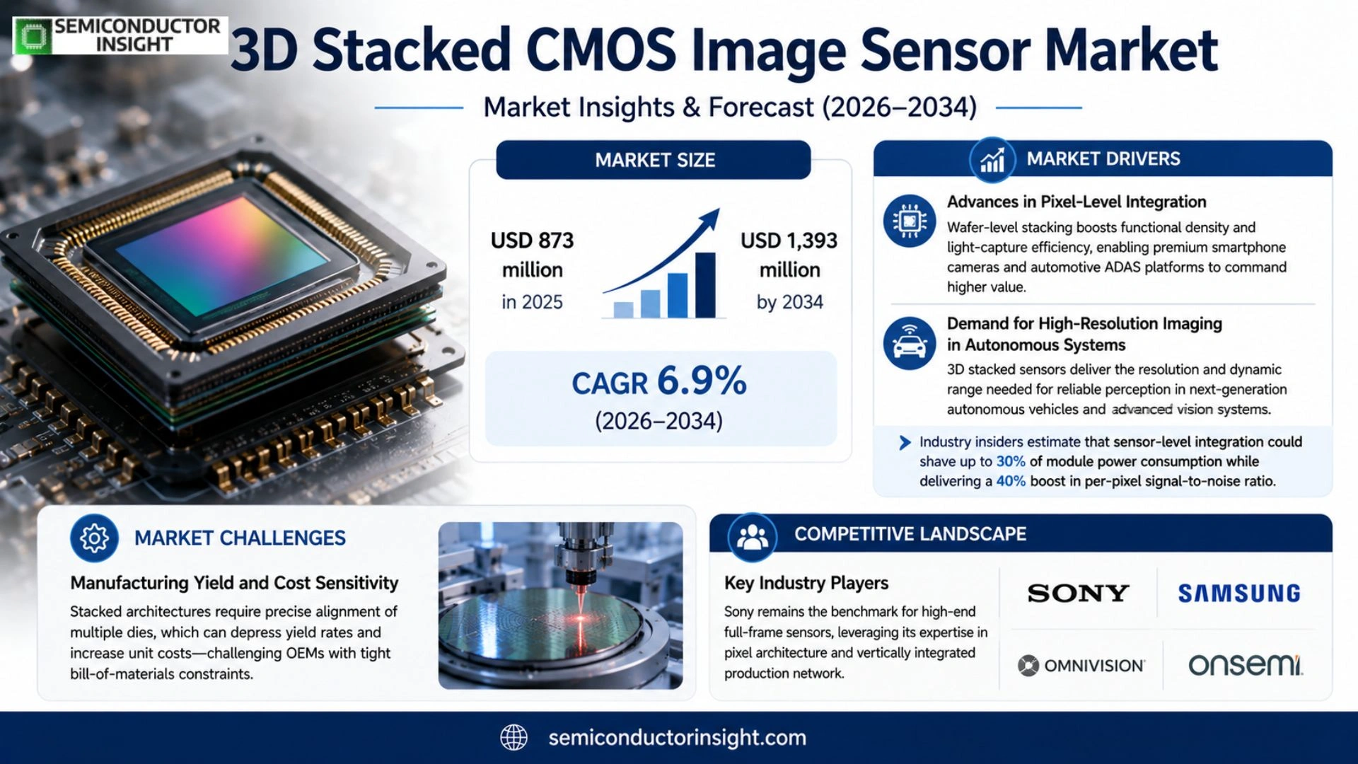
Global 3D Stacked CMOS Image Sensor market size was valued at USD 873 million in 2025. The market is forecasted to increase to USD 1,393 million by 2034, reflecting a CAGR of 6.9% over the period.
3D Stacked CMOS Image Sensor is an advanced image sensor that vertically stacks two or more semiconductor wafers,photosensitive layer, circuit layer and functional layer,using through‑silicon vias (TSVs) or hybrid bonding. By separating the light‑capture area from signal‑processing circuitry, each layer can be optimized independently, boosting light sensitivity, data‑transfer speed and integration density while lowering power consumption.
The demand rises because professional imaging equipment is being upgraded, industrial measurement and medical diagnostic systems require higher performance, and aerospace applications seek high‑speed high‑definition imaging. Opportunities exist in improving stacking yields, embedding intelligent processing in functional layers and developing global‑shutter compatible products. Leading manufacturers such as Sony, Samsung, OmniVision Technologies and STMicroelectronics are expanding portfolios to capture high‑value segments.
MARKET DRIVERS
Advances in Pixel‑Level Integration
3D Stacked CMOS Image Sensor Market is gaining traction as semiconductor manufacturers perfect wafer‑level stacking techniques that double the functional density without expanding the footprint. This integration enables superior light‑capture efficiency, a factor that is particularly valuable for premium smartphone cameras and automotive ADAS platforms. Companies that master this process can command higher price points, prompting accelerated R&D investment across the value chain.
Demand for High‑Resolution Imaging in Autonomous Systems
Automakers are embedding increasingly sophisticated vision stacks into next‑generation vehicles, and 3D Stacked CMOS Image Sensor Market supplies the resolution and dynamic‑range required for reliable perception under varied lighting. As OEMs shift from assisted to fully autonomous driving, sensor suppliers that can offer compact, power‑efficient stacks stand to secure long‑term design wins.
➤ Industry insiders estimate that sensor‑level integration could shave up to 30 % of module power consumption while delivering a 40 % boost in per‑pixel signal‑to‑noise ratio.
Beyond automotive, the push for augmented‑reality headsets and high‑definition surveillance drives a cross‑segment appetite for sensors that combine depth perception with low‑light performance, reinforcing the upward momentum in 3D Stacked CMOS Image Sensor Market.
MARKET CHALLENGES
Manufacturing Yield and Cost Sensitivity
Stacked architectures demand precise alignment of multiple dies, a step that historically depresses yield rates. The added process complexity translates into higher unit costs, which can deter OEMs operating under tight bill‑of‑materials constraints, especially in volume‑driven consumer electronics.
Other Challenges
Supply‑Chain Fragility
The reliance on advanced lithography equipment and specialized bonding tools creates a bottleneck; any disruption in equipment availability can cascade into delayed product launches and inventory shortages.
Regulatory Hurdles
Emerging safety standards for automotive vision systems impose strict validation protocols. Compliance testing adds both time and expense, forcing sensor vendors to invest in certification infrastructure before they can access high‑margin markets.
MARKET RESTRAINTS
Capital‑Intensive Tooling
Entry into 3D Stacked CMOS Image Sensor Market requires fabs to acquire expensive bonding equipment and to retrofit cleanrooms for multi‑die processing. Smaller players often lack the financial bandwidth to make such investments, limiting market concentration to a handful of well‑capitalized firms.
MARKET OPPORTUNITIES
Emerging Applications in Edge AI Devices
Edge AI workloads,ranging from smart industrial cameras to portable medical scanners,benefit from the high bandwidth and low latency that stacked sensors provide. As AI inference moves closer to the sensor plane, developers are seeking compact, power‑savvy imagers, opening a niche where early adopters can secure differentiated product portfolios.
Expansion into 5‑G+ Connectivity Ecosystems
The rollout of dense 5‑G networks creates demand for IoT nodes equipped with high‑fidelity vision, particularly in smart‑city deployments. Leveraging stacked CMOS technology enables these nodes to operate on limited energy budgets while transmitting richer visual data, positioning suppliers to capture a growing slice of the connectivity market.
3D Stacked CMOS Image Sensor Market Trends
Integration of Advanced Stacking Techniques
The industry is witnessing a swift shift toward multi‑layer architectures that separate the photosensitive tier from the processing circuitry. By employing through‑silicon vias and hybrid bonding, manufacturers can tailor each layer for optimal light capture, signal conversion, and on‑chip computation. This separation not only lifts quantum efficiency but also frees designers from the pixel‑pitch constraints that hamper conventional front‑ and back‑illuminated sensors. The result is a sharper signal‑to‑noise ratio, higher frame rates, and a reduced footprint that aligns with the miniaturisation agenda of premium imaging equipment. For OEMs, the ability to embed more functionality without expanding die size translates into lower bill‑of‑materials and improved thermal performance, a combination that strengthens the competitive positioning of products built on 3D Stacked CMOS Image Sensor Market.
Other Trends
Emergence of AI‑Enabled Functional Layers
Manufacturers are beginning to embed dedicated artificial‑intelligence processors within the stack, creating a third or fourth functional tier that handles on‑sensor analytics. This development satisfies the rising demand for edge‑computing capabilities in autonomous vehicles and smart factories, where latency penalties of off‑chip processing are unacceptable. By integrating AI kernels directly beneath the photodiode array, the sensor can pre‑filter noise, recognise patterns, and even execute basic classification tasks before transmitting data. This not only conserves bandwidth but also opens new revenue streams for vendors that can offer turnkey smart‑imaging modules rather than raw sensor chips.
Expansion into High‑Performance Industrial Applications
Industrial measurement and medical diagnostics are adopting 3D Stacked CMOS Image Sensor Market to meet stringent accuracy and speed requirements. High‑resolution, low‑noise capture is essential for precision metrology, while the ability to operate at elevated frame rates supports real‑time defect detection on assembly lines. In medical imaging, the reduced power draw and compact form factor enable portable endoscopic systems that retain desktop‑class image quality. Companies that refine stacking yields and enhance wafer‑level reliability are positioned to capture premium contracts in these sectors, where the cost of failure outweighs the premium price of advanced sensors.
COMPETITIVE LANDSCAPE
Key Industry Players
Competitive Overview of Global 3D Stacked CMOS Image Sensor Suppliers
Among the manufacturers, Sony remains the benchmark for high‑end full‑frame sensors, capitalising on its long‑standing expertise in pixel architecture and its vertically integrated production network. By isolating the photosensitive tier from the processing tier, Sony has been able to push quantum efficiency and read‑out speed beyond the limits of conventional BSI devices, securing a dominant share of premium camera modules used in professional photography and cinema. Its strategic investments in TSV and hybrid‑bonding facilities have translated into superior yields, meaning that customers seeking the utmost image fidelity consistently turn to Sony’s stacked offerings.
Beyond Sony, the market exhibits a diverse set of contenders that specialise in distinct niches. Samsung leverages its massive wafer capacity to supply volume‑driven automotive and consumer‑electronics segments, while OmniVision targets compact‑module applications through aggressive cost‑optimisation of dual‑layer stacks. STMicroelectronics and ON Semiconductor focus on industrial‑measurement and medical‑imaging sensors, integrating safety‑critical functions into the lower layers. SK Hynix and SmartSens are expanding their product lines with multi‑functional AI processing layers, aiming at edge‑compute imaging devices. Canon, Panasonic and Himax each maintain a portfolio of specialised sensors for surveillance and aerospace applications, and emerging players such as Toshiba, ROHM and Visionox are experimenting with wafer‑level bonding to lower production overhead and accelerate time‑to‑market.
List of Key 3D Stacked CMOS Image Sensor Companies Profiled
- Sony Corporation
- Samsung Electronics
- OmniVision Technologies
- STMicroelectronics
- ON Semiconductor
- SK Hynix Inc.
- SmartSens
- Canon Inc.
- Panasonic Corporation
- Himax Technologies
- Toshiba Electronic Devices & Storage
- ROHM Semiconductor
- Visionox
- e2v (Teledyne)
- Globalfoundries
Segment Analysis:
| Segment Category | Sub-Segments | Key Insights |
| By Type |
|
Multi‑Layer Stacked is emerging as the most compelling architecture because:
|
| By Application |
|
Automotive Electronics drives adoption through:
|
| By End User |
|
Professional Imaging benefits from:
|
| By Bonding Technology |
|
Hybrid Bonding is gaining traction because:
|
| By Functional Layer Integration |
|
AI Processing Layer Integrated Stacked Sensor delivers strategic advantage by:
|
Regional Analysis: 3D Stacked CMOS Image Sensor Market
Asia‑Pacific
Foundries in Taiwan and South Korea have expanded their 200‑mm and 300‑mm lines to accommodate wafer‑stacking steps, allowing higher yields for dual‑pixel arrays. The capacity boost is matched by tighter process control, which translates into more consistent image quality for automotive cameras.
Regional research institutes collaborate with chip makers on through‑silicon‑via (TSV) techniques that lower interconnect resistance. These joint projects accelerate the rollout of sensors that combine depth sensing and hyperspectral imaging on a single stack.
Proximity of component suppliers,lens modules, ASICs, and packaging firms,creates a just‑in‑time network, reducing inventory costs and enabling rapid model refresh cycles for consumer devices.
Rapid uptake in flagship smartphones and emerging AR/VR headsets fuels demand for compact, high‑dynamic‑range sensors, prompting OEMs to prioritize stacked architectures over legacy planar designs.
North America
North America remains a hub for system‑level integration, where camera module assemblers combine stacked sensors with advanced image signal processors. The region’s strength lies in software‑driven features,computational photography, AI‑enhanced low‑light performance,that demand sensors with deep pixel stacks. Although domestic fabrication is limited, partnerships with Asia‑Pacific fabs are deepening, allowing U.S. firms to secure supply while influencing roadmap specifications. The strategic focus on automotive driver‑monitoring systems also introduces new volume streams that require robust, stacked imaging solutions.
Europe
European activity concentrates on industrial and medical imaging, where regulatory scrutiny pushes firms toward highly reliable 3D stacked sensors. German and French equipment manufacturers are embedding stacked chips into precision inspection tools, capitalizing on the technology’s ability to deliver high‑resolution depth maps. Collaborative research programs funded by the EU accelerate standardization of bonding processes, which in turn lowers entry barriers for niche players and cultivates a specialized supplier base distinct from the consumer‑focused Asia‑Pacific market.
South America
In South America, the market is still nascent, but growing interest from telecom operators seeking to upgrade network‑enabled cameras drives modest demand. Countries such as Brazil are leveraging regional trade agreements to import stacked sensors at favorable terms, enabling local OEMs to prototype smarter surveillance solutions. The incremental adoption is fostering a small but skilled workforce that could support downstream assembly activities as the regional value chain matures.
Middle East & Africa
The Middle East & Africa region is predominantly driven by defense and border‑security projects that require rugged, high‑resolution imaging platforms. Suppliers are attracted by long‑term procurement contracts from government agencies, prompting them to offer customized stacked sensor packages that endure extreme temperatures. While local design capability remains limited, joint ventures with Asian manufacturers are emerging, laying the groundwork for future indigenous development of advanced imaging modules.
Report Scope
This market research report provides a comprehensive analysis of the 3D Stacked CMOS Image Sensor Market , covering the forecast period 2026–2034. It offers detailed insights into market dynamics, technological advancements, competitive landscape, and key trends shaping the industry.
Key focus areas of the report include:
- Market Overview: The report begins with an overview outlining its current market scenario, key growth indicators, and industry transformation drivers. It discusses macroeconomic factors, demand–supply balance, regulatory landscape, and the strategic role of semiconductors in powering advancements across industries such as automotive, telecommunications, consumer electronics, and industrial automation.
- Market Size & Forecast: Historical data and future projections for revenue, unit shipments, and market value across major regions and segments.
- Segmentation Analysis: Detailed breakdown by product type, technology, application, and end-user industry to identify high-growth segments and investment opportunities.
- Regional Insights: Insights into market performance across North America, Europe, Asia-Pacific, Latin America, and the Middle East & Africa, including country-level analysis where relevant.
- Competitive Landscape: Profiles of leading market participants, including their product offerings, R&D focus, manufacturing capacity, pricing strategies, and recent developments such as mergers, acquisitions, and partnerships.
- Technology Trends & Innovation: Assessment of emerging technologies, integration of AI/IoT, semiconductor design trends, fabrication techniques, and evolving industry standards.
- Market Drivers & Restraints: Evaluation of factors driving market growth along with challenges, supply chain constraints, regulatory issues, and market-entry barriers.
- Stakeholder Insights: Insights for component suppliers, OEMs, system integrators, investors, and policymakers regarding the evolving ecosystem and strategic opportunities.
Primary and secondary research methods are employed, including interviews with industry experts, data from verified sources, and real-time market intelligence to ensure the accuracy and reliability of the insights presented.
FREQUENTLY ASKED QUESTIONS:
What is the current market size of 3D Stacked CMOS Image Sensor Market?
-> 3D Stacked CMOS Image Sensor market is forecasted to increase to USD 1,393 million by 2034, reflecting a CAGR of 6.9% over the period.
Which key companies operate in 3D Stacked CMOS Image Sensor Market?
-> Key players include Sony, Samsung, OmniVision Technologies, STMicroelectronics, Onsemi, SK Hynix, SmartSens, and Canon, among others.
What are the key growth drivers?
-> Growth is driven by the upgrading of professional imaging equipment, rising demand for high‑performance sensors in industrial measurement and medical diagnosis, and expanding applications of high‑speed, high‑definition imaging in aerospace and other high‑value sectors.
Which region dominates the market?
-> The Asia region is projected to command the largest market share, supported by strong demand in consumer electronics, automotive electronics, and industrial measurement applications.
What are the emerging trends?
-> Emerging trends include the integration of AI processing layers, development of global‑shutter compatible sensors for high‑speed detection, and cost‑effective stacking solutions to broaden adoption into mid‑range applications.

Get Sample Report PDF for Exclusive Insights
Report Sample Includes
- Table of Contents
- List of Tables & Figures
- Charts, Research Methodology, and more...