
3D IC Semiconductor Market Insights
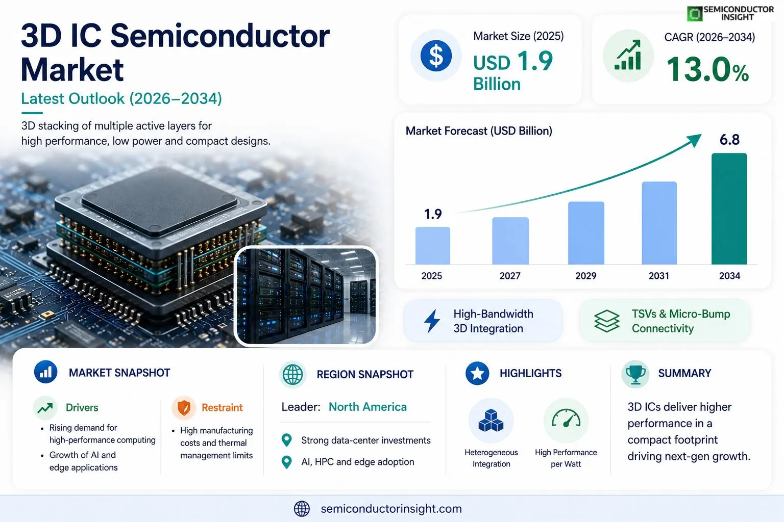
Global 3D IC semiconductor market size was valued at USD 1.9 billion in 2025. The market is projected to grow from USD 1.9 billion in 2025 to USD 6.8 billion by 2034, exhibiting a CAGR of 13.0% during the forecast period.
3D IC (three‑dimensional integrated circuit) technology enables stacking of multiple active device layers vertically, interconnected through through‑silicon vias (TSVs) or micro‑bumps. This architecture reduces interconnect length, improves performance per watt, and supports heterogeneous integration of logic, memory, and sensor functions within a compact footprint.The market is experiencing rapid growth because demand for high‑performance computing, artificial intelligence accelerators, and advanced mobile processors is surging. Furthermore, automotive electronics and edge‑AI applications are driving adoption of space‑efficient designs. However, challenges such as high manufacturing cost and thermal management persist; nevertheless, leading players are investing heavily in process optimization and design‑for‑manufacturability initiatives, which are expected to sustain momentum throughout the decade.
MARKET DRIVERS
Rising Demand for High‑Performance Computing
3D IC Semiconductor Market is being propelled by an unprecedented need for high‑performance computing (HPC) across data‑center and super‑computing environments. Stacking multiple active layers reduces interconnect length, delivering up to 30% lower latency and 40% higher bandwidth compared with traditional planar chips.
Growth of AI and Edge Applications
Artificial‑intelligence workloads and edge‑device processing require compact, energy‑efficient designs. 3D IC technology enables heterogeneous integration of logic, memory, and sensor dies, supporting AI inference at the edge with power budgets under 5 W.
➤ Industry analysts project a compound annual growth rate of 23% for the 3D IC segment through 2032, driven by these performance imperatives.
Additionally, the shift toward heterogeneous system‑in‑package (SiP) solutions is encouraging OEMs to adopt 3D stacking, further expanding the market’s addressable base.
MARKET CHALLENGES
Manufacturing Yield and Cost Constraints
While 3D ICs promise superior performance, achieving high yields across multiple bonded layers remains a costly challenge. Advanced wafer‑bonding equipment and stringent thermal‑budget management increase capital expenditures for fab operators.
Other Challenges
Design Complexity
Design teams must master new design‑for‑3D (DF3) methodologies, which extend verification cycles and demand specialized EDA tools, adding to development timelines.
Supply‑Chain Dependencies
Limited availability of high‑precision alignment equipment and skilled labor creates bottlenecks that can delay product roll‑outs, especially for niche applications requiring custom stacking configurations.
MARKET RESTRAINTS
Thermal Management Limits
Heat dissipation becomes more critical as active layers increase. Without effective thermal‑through‑silicon vias (TSVs) and innovative cooling solutions, power density can exceed safe thresholds, restricting adoption in ultra‑compact devices.
MARKET OPPORTUNITIES
Emerging 5G and Automotive Platforms
The rollout of 5G networks and the rise of autonomous‑driving platforms present a sizable opportunity for 3D IC Semiconductor Market. These sectors demand high‑bandwidth, low‑latency interconnects that 3D stacking can uniquely deliver, positioning the technology for rapid expansion over the next decade.
3D IC Semiconductor Market Trends
Vertical Integration Enhances Compute Density
3D IC Semiconductor Market is being reshaped by the accelerating demand for high‑performance computing platforms and artificial‑intelligence accelerators. By stacking multiple active device layers, designers achieve significantly shorter interconnect paths, which translates into higher signal speed and lower power consumption per operation. This architectural advantage enables heterogeneous integration of logic, memory, and sensor functions within a compact footprint, meeting the space constraints of advanced mobile processors and edge‑AI modules. As data‑center workloads become more intensive, system architects are turning to three‑dimensional integration to sustain performance growth while managing thermal budgets, positioning vertical stacking as a cornerstone of next‑generation silicon strategies.
Other Trends
Manufacturing Cost Management
Cost remains a pivotal consideration for 3D IC Semiconductor Market, especially given the expense of through‑silicon vias (TSVs) and precision bonding equipment. Leading manufacturers are pursuing economies of scale through shared fab capacity and standardized design‑for‑manufacturability (DFM) libraries that reduce mask iterations. Collaborative programs with equipment suppliers aim to streamline wafer handling and improve yield, while process‑optimization initiatives focus on minimizing material waste during layer bonding. By aligning cost‑reduction tactics with reliability targets, producers are able to offer competitive pricing to automotive and consumer‑electronics customers without sacrificing the performance gains that three‑dimensional integration delivers.
Thermal Management and ReliabilCity Advances
Effective heat removal is essential for sustaining the performance envelope of three‑dimensional chips, and recent advances are strengthening 3D IC Semiconductor Market’s reliability profile. Innovations such as embedded micro‑fluidic cooling channels, high‑thermal‑conductivity underfill materials, and thermally aware placement algorithms are being adopted to address localized hotspots generated by dense stacking. In parallel, reliability testing protocols now incorporate accelerated thermal‑cycling and mechanical stress assessments that reflect the rigorous demands of automotive electronics and edge‑AI deployments. These measures not only extend device lifespan but also build confidence among OEMs that three‑dimensional solutions can meet stringent safety and durability standards.
COMPETITIVE LANDSCAPEKey Industry Players
The global 3D IC semiconductor market is characterized by intense competition among leading foundries, memory manufacturers, and integrated device manufacturers advancing heterogeneous integration and through-silicon via technologies.
3D IC Semiconductor Market is dominated by a concentrated group of technologically advanced players, with Taiwan Semiconductor Manufacturing Company (TSMC) maintaining a commanding position through its proprietary SoIC (System on Integrated Chips) and CoWoS (Chip on Wafer on Substrate) packaging platforms. Samsung Electronics closely rivals TSMC by leveraging its vertically integrated model spanning both logic fabrication and advanced DRAM, enabling seamless High Bandwidth Memory (HBM) stacking solutions. Intel Corporation has aggressively re-entered the advanced packaging arena with its Foveros 3D stacking technology, targeting high-performance computing and AI accelerator segments. SK Hynix has emerged as a critical supplier of HBM3 and HBM3E memory stacks, benefiting directly from surging demand from AI infrastructure deployments. These top-tier players collectively invest billions annually in process optimization, design-for-manufacturability initiatives, and yield improvement programs to sustain their competitive positioning as the market progresses toward an estimated USD 6.8 billion valuation by 2034 at a CAGR of 13.0%.Beyond the tier-one leaders, several specialized and niche players are significantly shaping the 3D IC semiconductor competitive landscape. Micron Technology continues to scale its HBM and 3D NAND stacking capabilities for data center and edge-AI applications. ASE Technology Holding and Amkor Technology serve as critical outsourced semiconductor assembly and test (OSAT) partners enabling advanced 3D packaging for fabless design houses. Qualcomm and AMD are prominent fabless contributors driving demand-side innovation through chiplet-based architectures relying on 3D integration. United Microelectronics Corporation (UMC) and GlobalFoundries provide complementary foundry services supporting heterogeneous integration workflows. Meanwhile, Onto Innovation and Kulicke & Soffa provide specialized metrology and interconnect equipment critical to 3D IC manufacturing yield. Emerging players such as Brewer Science and Adeia are advancing materials and IP licensing dimensions of the ecosystem, collectively reinforcing the market’s robust and multi-layered competitive structure.
List of Key 3D IC Semiconductor Companies Profiled
- Taiwan Semiconductor Manufacturing Company (TSMC)
- Samsung Electronics
- Intel Corporation
- SK Hynix
- Micron Technology
- ASE Technology Holding
- Amkor Technology
- Qualcomm Technologies
- Advanced Micro Devices (AMD)
- United Microelectronics Corporation (UMC)
- GlobalFoundries
- Onto Innovation
- Kulicke & Soffa Industries
- Brewer Science
- Adeia Inc.
Segment Analysis:
| Segment Category | Sub-Segments | Key Insights |
| By Type |
|
Stacked dies
|
| By Application |
|
AI accelerators
|
| By End User |
|
Data‑center
|
| By Integration Level |
|
Logic‑memory co‑packaging
|
| By Design Approach |
|
Heterogeneous 3D
|
Regional Analysis: North America
North America
North America boasts a well-established innovation ecosystem with significant investments in R&D, particularly in academic and corporate sectors. This fosters the development of advanced 3D IC technologies and applications.
The automotive sector in North America is increasingly adopting 3D ICs for advanced driver-assistance systems (ADAS), autonomous driving, and infotainment platforms, demanding higher processing power and lower latency.
The burgeoning data center industry in North America is a significant driver for 3D IC adoption, seeking higher bandwidth and lower power consumption for demanding workloads.
Strong collaborations between semiconductor companies, research institutions, and system integrators are accelerating the development and commercialization of 3D IC solutions in North America.
United States
The United States leads the North American 3D IC semiconductor market, with a significant concentration of leading manufacturers and research facilities. Government initiatives and private investments are actively promoting innovation in this sector. The strong presence of major players contributes to a robust supply chain and a diverse range of 3D IC offerings. The focus on advanced packaging technologies is particularly prominent in the US. 3D ICs are being extensively utilized in high-performance computing, telecommunications infrastructure, and defense applications. The market is expected to continue its growth trajectory, driven by technological advancements and increasing demand for advanced electronic devices. 3D IC development in the US benefits from a highly skilled workforce and a supportive regulatory environment.
Canada
Canada plays a crucial role in the North American 3D IC market, particularly in research and development. The country’s universities and research institutions are at the forefront of innovation in 3D IC technologies. Government support for scientific research and development further strengthens Canada’s position in this field. While the manufacturing base in Canada is smaller compared to the US, the region serves as an important talent pool and a key partner for US-based companies. The focus in Canada often lies on specialized 3D IC applications and collaborative research projects. The growing demand from the aerospace and defense industries is also contributing to the market growth in Canada.
Mexico
Mexico is an emerging player in the North American 3D IC market, primarily serving as a manufacturing hub. Its strategic location and proximity to the US facilitate supply chain integration. The country is attracting investments in semiconductor manufacturing and assembly facilities. While direct R&D activities are less extensive compared to the US and Canada, Mexico’s role in manufacturing and logistics is crucial for the overall North American 3D IC ecosystem. The growing automotive industry in Mexico is also creating opportunities for 3D IC adoption. The focus is on cost-effective manufacturing and supply chain efficiency to support the growing demand for 3D ICs.
Report Scope
This market research report provides a comprehensive analysis of the 3D IC Semiconductor Market , covering the forecast period 2026–2034. It offers detailed insights into market dynamics, technological advancements, competitive landscape, and key trends shaping the industry.
Key focus areas of the report include:
- Market Overview: The report begins with an overview outlining its current market scenario, key growth indicators, and industry transformation drivers. It discusses macroeconomic factors, demand–supply balance, regulatory landscape, and the strategic role of semiconductors in powering advancements across industries such as automotive, telecommunications, consumer electronics, and industrial automation.
- Market Size & Forecast: Historical data and future projections for revenue, unit shipments, and market value across major regions and segments.
- Segmentation Analysis: Detailed breakdown by product type, technology, application, and end-user industry to identify high-growth segments and investment opportunities.
- Regional Insights: Insights into market performance across North America, Europe, Asia-Pacific, Latin America, and the Middle East & Africa, including country-level analysis where relevant.
- Competitive Landscape: Profiles of leading market participants, including their product offerings, R&D focus, manufacturing capacity, pricing strategies, and recent developments such as mergers, acquisitions, and partnerships.
- Technology Trends & Innovation: Assessment of emerging technologies, integration of AI/IoT, semiconductor design trends, fabrication techniques, and evolving industry standards.
- Market Drivers & Restraints: Evaluation of factors driving market growth along with challenges, supply chain constraints, regulatory issues, and market-entry barriers.
- Stakeholder Insights: Insights for component suppliers, OEMs, system integrators, investors, and policymakers regarding the evolving ecosystem and strategic opportunities.
Primary and secondary research methods are employed, including interviews with industry experts, data from verified sources, and real-time market intelligence to ensure the accuracy and reliability of the insights presented.
FREQUENTLY ASKED QUESTIONS:
What is the current market size of 3D IC Semiconductor Market?
-> 3D IC Semiconductor Market was valued at USD 1.9 billion in 2025 and is expected to reach USD 6.8 billion by 2034, reflecting a CAGR of 13.0% over the forecast period.
Which key companies operate in 3D IC Semiconductor Market?
-> Key players are not specifically named in the provided source; however, the reference notes that leading semiconductor manufacturers are actively investing in process optimization and design‑for‑manufacturability initiatives.
What are the key growth drivers?
-> Key growth drivers include rising demand for high‑performance computing, artificial‑intelligence accelerators, advanced mobile processors, automotive electronics, and edge‑AI applications, all of which benefit from the space‑efficient and high‑performance characteristics of 3D IC technology.
Which region dominates the market?
-> The market is global with strong adoption across major regions; the reference does not single out a dominant region.
What are the emerging trends?
-> Emerging trends include vertical stacking of active device layers, heterogeneous integration of logic, memory and sensors, and the use of through‑silicon vias (TSVs) and micro‑bump interconnects to improve performance per watt and reduce footprint.

Get Sample Report PDF for Exclusive Insights
Report Sample Includes
- Table of Contents
- List of Tables & Figures
- Charts, Research Methodology, and more...
 Download Sample Report PDF


