
3D Hybrid Bonding for AI Logic-Memory Stack Market Insights
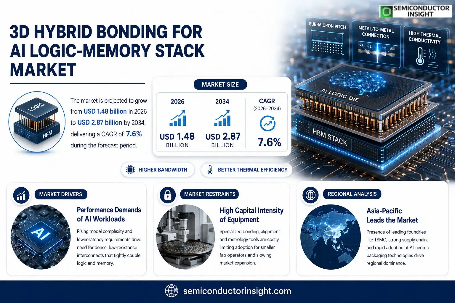
3D Hybrid Bonding for AI Logic-Memory Stack market measured USD 1.42 billion in 2025. It will climb from USD 1.48 billion in 2026 to USD 2.87 billion by 2034, delivering a compound annual growth rate of about 7.6 % over the period.
3D hybrid bonding refers to a wafer-level interconnect process that creates direct metal-to-metal contacts between stacked silicon dies, eliminating traditional solder bumps or adhesive layers. The technique enables sub-micron pitch interconnects and high thermal conductivity, which are essential for tightly coupling AI logic cores with high-bandwidth memory stacks.The upward trajectory reflects several forces: increasing adoption of AI inference chips that require dense logic-memory integration; cost pressures pushing manufacturers toward higher yields offered by defect-tolerant bonding; and ongoing investments in advanced packaging infrastructure across major foundries. Recent moves illustrate this momentumfor example, TSMC announced expanded capacity for its CoWoS® platform incorporating hybrid bonding in early 2024, while Intel disclosed a partnership with ASE Group aimed at scaling hybrid-bonded memory stacks for next-generation Xeon processors.
MARKET DRIVERS
Performance Demands of AI Workloads
The relentless push for larger model parameters and lower inference latency forces chip designers to seek interlayer connections that add negligible resistance while delivering sub‑micron pitch. 3D Hybrid Bonding for AI Logic‑Memory Stack Market offers a physical pathway that tightly couples compute and storage, thereby shaving nanoseconds from critical data‑move cycles.
Advances in Interconnect Technology
Recent breakthroughs in wafer‑level alignment and low‑temperature metal activation have reduced defect rates, making hybrid bonding a credible alternative to traditional TSV approaches. This progress translates into higher bandwidth per square millimeter, a metric that many AI silicon roadmaps now treat as a primary success factor.
➤ Analysts observe that early adopters of hybrid bonding are already recording up to a 20% improvement in overall system throughput compared with conventional stacking techniques.
Beyond raw speed, the thermal profile of stacked die benefits from the thinner interconnect stack, enabling more aggressive clocking without triggering hot‑spot alarms. Vendors that integrate hybrid bonding can therefore position their products as both faster and more reliable.
MARKET CHALLENGES
Thermal Management Constraints
Even with a slimmer interconnect stack, the dense placement of AI cores intensifies heat generation. Cooling solutions must evolve in tandem, as excessive temperature gradients can deteriorate bond integrity over time. Companies that overlook this coupling risk premature failure in high‑performance servers.
Other Challenges
Manufacturing Yield
Achieving consistent yield across large wafers remains a hurdle; minute particle contamination or alignment errors can cascade into costly rework cycles. The industry is therefore investing heavily in inline inspection tools to safeguard throughput.
MARKET RESTRAINTS
Capital Intensity of Equipment
The transition to hybrid bonding necessitates a suite of specialized deposition, bonding, and metrology equipment that can strain capital budgets, especially for midsize fab operators. Without access to financing or shared‑use facilities, some players may defer adoption, tempering overall market velocity.
MARKET OPPORTUNITIES
Emerging Data Center Architectures
Modular, composable data centers are seeking ultra‑low‑latency memory pathways to support edge AI inference. Hybrid‑bonded logic‑memory stacks fit naturally into these designs, offering a compact form factor that reduces board‑level routing complexity. Service providers that embed such stacks can differentiate their offerings on both performance and power efficiency, unlocking a fresh revenue stream for equipment suppliers.
3D Hybrid Bonding for AI Logic-Memory Stack Market Trends
AI Inference Chip Integration Fuels Hybrid Bonding Uptake
The transition from discrete logic and memory modules toward tightly coupled AI inference engines has reshaped packaging priorities. Engineers now require interconnects that can sustain sub‑micron pitches while exporting heat efficiently, because AI workloads generate dense switching activity at the chip‑level. 3D hybrid bonding supplies a metal‑to‑metal interface that eliminates solder bumps, thereby shrinking the vertical stack height and reducing thermal resistance. This technical advantage translates into higher bandwidth per pin and more predictable performance under the aggressive power envelopes typical of modern AI accelerators. As design houses prioritize these attributes, the adoption curve for hybrid‑bonded stacks accelerates, prompting supply‑chain participants to align their roadmaps with the emerging logic‑memory convergence.
Other Trends
Yield Enhancement Through Defect‑Tolerant Processes
Manufacturers face mounting pressure to improve wafer utilization as feature sizes shrink. Hybrid bonding’s ability to accommodate minor surface irregularities allows a larger fraction of dies to meet qualification thresholds. Consequently, fab managers report noticeable gains in effective yield when substituting traditional micro‑bump assemblies with hybrid interfaces. The improvement eases pricing pressure on AI‑centric products, because higher usable output per wafer reduces unit cost without sacrificing performance. This efficiency gain also encourages smaller foundries to enter the AI packaging arena, broadening the competitive landscape.
Foundry Capacity Expansion Strengthens Ecosystem
Strategic investments by leading foundries illustrate how the ecosystem is responding to the demand shift. Early in 2024, TSMC announced additional production lanes for its CoWoS® platform that now embed hybrid bonding as a standard option, effectively widening the design envelope for customers seeking high‑bandwidth memory integration. Simultaneously, Intel disclosed a collaborative effort with ASE Group to scale hybrid‑bonded memory stacks for next‑generation Xeon processors, signaling confidence that the technology can meet the throughput requirements of data‑center AI workloads. These moves not only increase the availability of qualified manufacturing slots but also generate a feedback loop: as more design houses target hybrid‑bonded architectures, equipment suppliers accelerate tooling upgrades, which in turn lowers entry barriers for additional participants. The cumulative effect is a more resilient supply chain that can sustain the pace of AI‑driven product cycles.
COMPETITIVE LANDSCAPEKey Industry Players
3D Hybrid Bonding Drives AI Logic‑Memory Stack Competitive Dynamics
The market is anchored by a handful of semiconductor giants that have translated packaging expertise into differentiated AI logic‑memory solutions. Taiwan Semiconductor Manufacturing Company (TSMC) leverages its CoWoS® platform to integrate hybrid‑bonded dies at scale, positioning the foundry as a primary supplier for AI accelerators that demand sub‑micron interconnect pitch and superior thermal paths. Intel’s recent alliance with ASE Group amplifies its ability to offer bundled logic‑memory stacks for next‑generation Xeon processors, blending in‑house design control with ASE’s proven bonding line. Samsung Electronics complements the rivalry by injecting massive volume capacity and by experimenting with heterogeneous integration that pairs its high‑bandwidth memory (HBM) offerings with custom AI logic. Meanwhile, Foundries has carved a niche by targeting cost‑sensitive applications, deploying defect‑tolerant hybrid bonding to improve yield without sacrificing performance. This concentration of capability creates a tiered ecosystem where the top tier supplies full‑stack services, while lower tiers focus on volume‑driven or specialty segments, thereby shaping partner selection and pricing power across the supply chain.Beyond the headline players, a diverse set of specialists enriches the competitive fabric. Amkor Technology and ASE Group (listed separately for its dual role as outsource assembler and partner) provide extensive packaging lines that enable smaller fabless firms to adopt hybrid bonding without building dedicated infrastructure. Micron Technology and SK Hynix, as memory‑centric OEMs, are increasingly packaging their DDR and HBM products directly onto AI logic dies, unlocking bandwidth gains that pure logic vendors cannot achieve alone. STMicroelectronics and NXP Semiconductors apply hybrid bonding to edge‑compute modules, where compact form factor and thermal efficiency are decisive. AMD, Fujitsu, and Renesas contribute niche ASICs and embedded processors that benefit from tighter logic‑memory coupling for inference workloads in automotive and industrial IoT. Broadcom’s focus on networking ASICs has prompted exploratory hybrid‑bonding pilots to reduce latency in data‑center switches. Collectively, these firms sustain a vibrant second tier that fuels innovation, pressures incumbents to refine cost structures, and expands the addressable market for AI‑optimized stacks.
List of Key 3D Hybrid Bonding for AI Logic-Memory Stack Companies Profiled
- TSMC
- Intel
- ASE Group
- Samsung Electronics
- Foundries
- Amkor Technology
- Micron Technology
- SK Hynix
- STMicroelectronics
- NXP Semiconductors
- AMD
- Fujitsu
- Renesas Electronics
- Broadcom Inc.
Segment Analysis:
| Segment Category | Sub-Segments | Key Insights |
| By Type |
|
Wafer‑to‑Wafer Hybrid Bonding
|
| By Application |
|
AI Inference Accelerators
|
| By End User |
|
Cloud Service Providers
|
| By Manufacturing Strategy |
|
Integrated Foundry‑Fab Partnerships
|
| By Performance Requirement |
|
Ultra‑Low‑Latency Interconnects
|
Regional Analysis: 3D Hybrid Bonding for AI Logic-Memory Stack Market
North America
The region benefits from a vertically integrated supply chain, where wafer fabs, assembly houses, and test facilities operate under coordinated quality standards, reducing lead times for hybrid‑bonded modules.
Recent export‑control revisions encourage domestic sourcing of critical bonding chemicals, accelerating the adoption of homegrown solutions for AI logic‑memory stacks.
A steady pipeline of engineers trained in 3D integration and AI architectures sustains innovation cycles, while cross‑border collaborations enrich design methodologies.
Enterprises deploying autonomous systems and high‑frequency trading platforms are prioritizing low‑power, high‑density stacks, driving early‑stage orders for hybrid‑bonded products.
Europe
European manufacturers are leveraging strong public‑private research consortia to validate 3D Hybrid Bonding for AI Logic-Memory Stack concepts within automotive and industrial IoT domains. Policy incentives aimed at semiconductor sovereignty have prompted investments in niche fab lines that specialize in heterogeneous stacking, allowing OEMs to certify safety‑critical modules locally. The continent’s fragmented market structure, however, creates a need for standardised interface specifications, an effort currently coordinated by the European Semiconductor Industry Association. As chip designers adopt more aggressive floor‑planning techniques, European fabs are positioning themselves as preferred partners for low‑volume, high‑mix production runs, offering flexibility that larger North American players cannot match.
Asia‑Pacific
Asia‑Pacific’s rapid scaling of foundry capacity translates into a competitive environment for 3D Hybrid Bonding for AI Logic-Memory Stack technologies. Leading fabs in Taiwan and South Korea are integrating hybrid bonding steps into their advanced nodes, driven by the region’s demand for AI accelerators in consumer electronics. Meanwhile, emerging hubs in Singapore and Malaysia are attracting design houses that value proximity to manufacturing and to a growing pool of materials‑science experts. The strategic emphasis on cost efficiency pushes suppliers to streamline bonding chemistries, which may influence pricing benchmarks. Nonetheless, intellectual‑property concerns remain a barrier for some Western firms considering joint ventures in the region.
South America
South America’s market remains modest but is showing signs of maturation as local governments launch incentive programs for high‑performance computing infrastructure. Brazil’s semiconductor cluster is beginning to explore hybrid‑bonded stack prototypes for climate‑modeling supercomputers, a niche that aligns with the country’s scientific agenda. The scarcity of dedicated fabs forces designers to partner with offshore foundries, yet the region’s growing expertise in packaging and test services creates an ancillary value chain that could support future domestic production. Market participants should monitor policy shifts that may unlock additional funding for research collaborations.
Middle East & Africa
In the Middle East & Africa, strategic investment in digital transformation is sparking early interest in 3D Hybrid Bonding for AI Logic-Memory Stack solutions, particularly within sovereign cloud initiatives. The United Arab Emirates has announced a dedicated fund for next‑generation chip manufacturing, aiming to attract technology transfer agreements with established players. African nations, while still nascent in semiconductor fabrication, are focusing on building robust design ecosystems that could eventually feed into hybrid‑bonding projects. The primary challenge lies in developing a skilled workforce and securing reliable supply lines for high‑purity bonding agents, a gap that international training programs are beginning to address.
Report Scope
This market research report provides a comprehensive analysis of the 3D Hybrid Bonding for AI Logic-Memory Stack Market , covering the forecast period 2026–2034. It offers detailed insights into market dynamics, technological advancements, competitive landscape, and key trends shaping the industry.
Key focus areas of the report include:
- Market Overview: The report begins with an overview outlining its current market scenario, key growth indicators, and industry transformation drivers. It discusses macroeconomic factors, demand–supply balance, regulatory landscape, and the strategic role of semiconductors in powering advancements across industries such as automotive, telecommunications, consumer electronics, and industrial automation.
- Market Size & Forecast: Historical data and future projections for revenue, unit shipments, and market value across major regions and segments.
- Segmentation Analysis: Detailed breakdown by product type, technology, application, and end-user industry to identify high-growth segments and investment opportunities.
- Regional Insights: Insights into market performance across North America, Europe, Asia-Pacific, Latin America, and the Middle East & Africa, including country-level analysis where relevant.
- Competitive Landscape: Profiles of leading market participants, including their product offerings, R&D focus, manufacturing capacity, pricing strategies, and recent developments such as mergers, acquisitions, and partnerships.
- Technology Trends & Innovation: Assessment of emerging technologies, integration of AI/IoT, semiconductor design trends, fabrication techniques, and evolving industry standards.
- Market Drivers & Restraints: Evaluation of factors driving market growth along with challenges, supply chain constraints, regulatory issues, and market-entry barriers.
- Stakeholder Insights: Insights for component suppliers, OEMs, system integrators, investors, and policymakers regarding the evolving ecosystem and strategic opportunities.
Primary and secondary research methods are employed, including interviews with industry experts, data from verified sources, and real-time market intelligence to ensure the accuracy and reliability of the insights presented.
FREQUENTLY ASKED QUESTIONS:
What is the current market size of 3D Hybrid Bonding for AI Logic-Memory Stack Market?
-> 3D Hybrid Bonding for AI Logic-Memory Stack Market was valued at USD 1.42 billion in 2025 and is expected to reach USD 2.87 billion by 2034, reflecting a compound annual growth rate of approximately 7.6 % over the forecast period.
Which key companies operate in 3D Hybrid Bonding for AI Logic-Memory Stack Market?
-> Key players include TSMC, Intel Corporation, ASE Group, and other leading advanced‑packaging specialists that are actively developing and scaling hybrid‑bonded memory stacks.
What are the key growth drivers?
-> Key growth drivers include rising demand for AI inference chips requiring dense logic‑memory integration, cost pressures driving defect‑tolerant bonding solutions, and continued investment in advanced packaging infrastructure by major foundries.
Which region dominates the market?
-> Asia‑Pacific leads the market, driven by the concentration of semiconductor foundries such as TSMC and the rapid adoption of AI‑centric packaging technologies in the region.
What are the emerging trends?
-> Emerging trends include expansion of CoWoS® platforms incorporating hybrid bonding, strategic partnerships to scale memory‑stack production (e.g., Intel‑ASE collaboration), and the development of next‑generation Xeon processors leveraging hybrid‑bonded stacks.
Get Sample Report PDF for Exclusive Insights
Report Sample Includes
- Table of Contents
- List of Tables & Figures
- Charts, Research Methodology, and more...
 Download Sample Report PDF





