
3D Chip Stacking Technology Market Insights
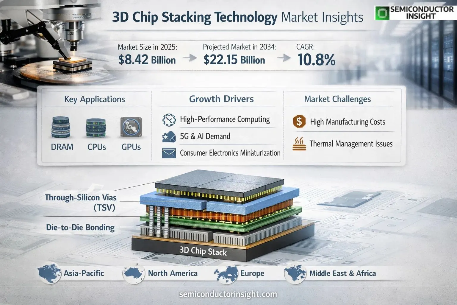
Global 3D chip stacking technology market size was valued at USD 8.42 billion in 2025. The market is projected to grow from USD 9.76 billion in 2026 to USD 22.15 billion by 2034, exhibiting a CAGR of 10.8% during the forecast period.
3D chip stacking technology enables vertical integration of semiconductor components, enhancing performance while reducing power consumption and footprint. This advanced packaging method utilizes techniques such as Through-Silicon Via (TSV), die-to-die bonding, and hybrid memory cubes to interconnect multiple layers of chips efficiently.
The market growth is driven by increasing demand for high-performance computing, AI applications, and miniaturization in consumer electronics. Leading players like TSMC, Samsung, and Intel are investing heavily in R&D to refine TSV and wafer-level packaging technologies. For instance, in Q1 2024, Samsung announced a breakthrough in ultra-thin interposer technology, enabling denser chip stacking for next-gen GPUs and data center processors.
MARKET DRIVERS
Increasing Demand for Compact Semiconductor Solutions
The 3D chip stacking technology market is driven by the growing need for high-performance, compact semiconductor solutions in consumer electronics and data centers. With 5G networks and AI applications demanding faster processing, 3D integration reduces latency while improving power efficiency. Market projections indicate a compound annual growth rate exceeding 20% for the next five years.
Advancements in Heterogeneous Integration
Breakthroughs in TSV (Through-Silicon Via) technology enable seamless integration of memory, logic, and sensor chips in vertical stacks. This innovation significantly improves data transfer speeds between components, making 3D chip stacking essential for next-generation computing architectures.
Automotive sector is projected to adopt 3D chip stacking at 25% higher rates by 2027 for advanced driver assistance systems (ADAS).
Leading semiconductor manufacturers are investing over $15 billion annually in 3D packaging R&D, signaling strong market confidence in this technology’s growth trajectory.
MARKET CHALLENGES
High Manufacturing Complexity and Costs
While 3D chip stacking offers performance benefits, the manufacturing process requires specialized equipment and cleanroom facilities that add 30-40% to production costs compared to traditional packaging methods. Yield management remains a critical challenge as defect rates in multi-layer stacks impact profitability.
Other Challenges
Thermal Management Issues
Heat dissipation becomes increasingly difficult with vertical chip stacking, requiring advanced cooling solutions that add to system complexity and cost. Maintaining thermal stability across multiple active layers reduces some of the performance advantages.
MARKET RESTRAINTS
Standardization and Compatibility Hurdles
The lack of universal design standards for 3D chip stacking creates interoperability challenges across different manufacturers’ solutions. Current ecosystem fragmentation limits widespread adoption, particularly in industries requiring long product lifecycles.
MARKET OPPORTUNITIES
Emerging Applications in Edge Computing
3D chip stacking technology is finding new growth opportunities in edge computing devices where space constraints demand high computational density. The market for edge AI chips using 3D integration is projected to reach $8 billion by 2026 as IoT deployments accelerate across industries.
3D Chip Stacking Technology Market Trends
Advancements in Through-Silicon Via (TSV) Technology
The 3D Chip Stacking Technology market is witnessing significant advancements in Through-Silicon Via (TSV) solutions, which enable vertical interconnects between stacked chips. Major semiconductor manufacturers are investing in TSV development to improve performance, reduce power consumption, and enhance thermal management in advanced packaging applications.
Other Trends
Adoption in High-Performance Computing
3D Chip Stacking Technology is increasingly being adopted in high-performance computing applications, including CPUs and GPUs. The technology’s ability to provide higher bandwidth and lower latency is driving demand in data centers and AI processing units.
Market Consolidation and Strategic Partnerships
The 3D Chip Stacking Technology market is experiencing consolidation, with leading players like TSMC, Samsung, and Intel forming strategic partnerships. These collaborations focus on developing standardized processes and improving yield rates in 3D chip stacking solutions.
Diversification Across Applications
Beyond traditional memory applications in DRAM, 3D Chip Stacking Technology is expanding into new areas including medical devices, automotive electronics, and IoT solutions. This diversification is creating new growth opportunities in the market.
Regional Market Developments
Asia-Pacific continues to dominate the 3D Chip Stacking Technology market, with significant investments from South Korea, Taiwan, and China. Meanwhile, North American and European markets are focusing on R&D for specialized applications in defense and aerospace sectors.
Die-to-Die Bonding Innovations
Recent developments in die-to-die bonding techniques are improving pad pitch scaling and interconnect density in 3D Chip Stacking Technology. These innovations are crucial for heterogeneous integration in next-generation semiconductor devices.
Manufacturing Efficiency Improvements
Industry leaders are implementing new wafer-level packaging techniques and testing methodologies to enhance manufacturing efficiency in 3D Chip Stacking Technology. These improvements are helping reduce costs while maintaining high reliability standards.
COMPETITIVE LANDSCAPE
Key Industry Players
Semiconductor Giants Drive Innovation in 3D Stacking Technology
The 3D chip stacking technology market is dominated by leading semiconductor manufacturers TSMC, Samsung, and Intel, collectively holding over 60% market share. These companies have pioneered Through-Silicon Via (TSV) technology and advanced packaging solutions, with TSMC notably developing its CoWoS (Chip on Wafer on Substrate) platform for high-performance computing applications. The market exhibits an oligopolistic structure with intensive R&D investments creating significant entry barriers.
Specialist players like ASE Technology and Amkor Technology provide crucial outsourced semiconductor assembly and test (OSAT) services, enabling flexible production scaling. Emerging innovators such as Xilinx (now part of AMD) are driving adoption in FPGA applications, while memory specialists Micron and SK Hynix lead in 3D-stacked DRAM implementations. The ecosystem also includes equipment suppliers like Applied Materials and ASML that enable advanced manufacturing capabilities.
List of Key 3D Chip Stacking Technology Companies Profiled
- TSMC
- Samsung Electronics
- Intel Corporation
- Micron Technology
- SK Hynix
- ASE Technology Holding
- Amkor Technology
- United Microelectronics Corporation (UMC)
- GlobalFoundries
- Xilinx (AMD)
- Toshiba Electronic Devices & Storage Corporation
- Applied Materials
- ASML Holding
- JCET Group
- Powertech Technology
Segment Analysis:
| Segment Category | Sub-Segments | Key Insights |
| By Type |
|
Through-Silicon Via (TSV) dominates the market due to its superior performance in high-density interconnects.
|
| By Application |
|
DRAM applications show strongest adoption of 3D stacking technology.
|
| By End User |
|
Data Center segment drives the most demand for advanced 3D stacking solutions.
|
| By Technology Node |
|
Below 7nm nodes are seeing the most aggressive adoption of 3D stacking.
|
| By Wafer Size |
|
300mm wafers dominate current 3D chip stacking production.
|
Regional Analysis: 3D Chip Stacking Technology Market
Asia-Pacific
TSMC’s proprietary Chip-on-Wafer-on-Substrate (CoWoS) technology sets industry benchmarks for 3D chip stacking yields. Their InFO-PoP solutions demonstrate superior thermal performance in mobile processors, attracting major smartphone OEMs to the region.
Samsung and SK Hynix are pioneering 3D-stacked memory architectures, with HBM3 production achieving 12-layer stack configurations. Their advanced TSV processes enable unprecedented bandwidth for AI/ML accelerators.
JCET and Tongfu Microelectronics are scaling advanced packaging capacity, with particular focus on fan-out wafer-level packaging (FO-WLP) compatibility with 3D chip stacking designs in 5G base stations.
Japanese suppliers like Shin-Etsu and Tokyo Electron provide critical thin-film dielectrics and bonding materials that enhance reliability in 3D stacked die configurations, particularly for automotive applications.
North America
The North American 3D chip stacking market thrives on AI accelerator demand, with NVIDIA, AMD and Intel driving interposer-based designs. Silicon Valley’s EDA tool dominance enables complex 3D IC floorplanning, while academic collaborations at institutions like Georgia Tech advance thermal management solutions. Defense contractors leverage 3D stacking for size-constrained aerospace electronics, creating specialized demand for radiation-hardened variants.
Europe
Europe’s 3D chip stacking adoption centers on automotive and industrial applications, with Infineon and STMicroelectronics developing robust stacking solutions for power electronics. Imec’s research consortium in Belgium accelerates EUV lithography integration for fine-pitch TSVs, while Germany’s Fraunhofer Institute pioneers chiplet-standardization initiatives crucial for heterogeneous integration.
Middle East & Africa
Emerging investments in smart city infrastructure are driving initial 3D chip stacking adoption for edge AI processors in the Gulf region. Abu Dhabi’s G42 is collaborating with international partners on stacked memory solutions for climate modeling supercomputers, while South Africa’s semiconductor test facilities are expanding capabilities for 3D IC validation.
South America
Brazil’s aerospace sector presents niche opportunities for 3D stacked ICs in satellite systems, with EMBRAER exploring radiation-tolerant designs. Chile’s astronomy infrastructure creates specialized demand for high-bandwidth stacked sensor arrays, though local manufacturing remains dependent on imported advanced packaging services.
Report Scope
This market research report provides a comprehensive analysis of the 3D Chip Stacking Technology Market, covering the forecast period 2025–2034. It offers detailed insights into market dynamics, technological advancements, competitive landscape, and key trends shaping the industry.
Key focus areas of the report include:
- Market Overview: The report begins with an overview outlining its current market scenario, key growth indicators, and industry transformation drivers. It discusses macroeconomic factors, demand–supply balance, regulatory landscape, and the strategic role of semiconductors in powering advancements across industries such as automotive, telecommunications, consumer electronics, and industrial automation.
- Market Size & Forecast: Historical data and future projections for revenue, unit shipments, and market value across major regions and segments.
- Segmentation Analysis: Detailed breakdown by product type, technology, application, and end-user industry to identify high-growth segments and investment opportunities.
- Regional Insights: Insights into market performance across North America, Europe, Asia-Pacific, Latin America, and the Middle East & Africa, including country-level analysis where relevant.
- Competitive Landscape: Profiles of leading market participants, including their product offerings, R&D focus, manufacturing capacity, pricing strategies, and recent developments such as mergers, acquisitions, and partnerships.
- Technology Trends & Innovation: Assessment of emerging technologies, integration of AI/IoT, semiconductor design trends, fabrication techniques, and evolving industry standards.
- Market Drivers & Restraints: Evaluation of factors driving market growth along with challenges, supply chain constraints, regulatory issues, and market-entry barriers.
- Stakeholder Insights: Insights for component suppliers, OEMs, system integrators, investors, and policymakers regarding the evolving ecosystem and strategic opportunities.
Primary and secondary research methods are employed, including interviews with industry experts, data from verified sources, and real-time market intelligence to ensure the accuracy and reliability of the insights presented.
FREQUENTLY ASKED QUESTIONS:
What is the current market size of 3D Chip Stacking Technology Market?
-> 3D Chip Stacking Technology Market was valued at USD million in 2025 and is expected to reach USD million by 2034.
Which key companies operate in 3D Chip Stacking Technology Market?
-> Key players include TSMC, Micron, SK Hynix, Samsung, Intel, ASE Technology, and Amkor Technology, among others.
What is the growth rate of Through-Silicon Via (TSV) segment?
-> The Through-Silicon Via (TSV) segment is projected to reach USD million by 2034, growing at a CAGR of % over the forecast period.
Which region leads in 3D Chip Stacking Technology adoption?
-> The U.S. market is estimated at USD million in 2025, while China is projected to reach USD million by 2034.
What are the main applications of 3D Chip Stacking Technology?
-> Key applications include DRAM, CPUs, GPUs, and others, with DRAM being a significant segment.
Get Sample Report PDF for Exclusive Insights
Report Sample Includes
- Table of Contents
- List of Tables & Figures
- Charts, Research Methodology, and more...
 Download Sample Report PDF




