2D Material Transistor Market Insights
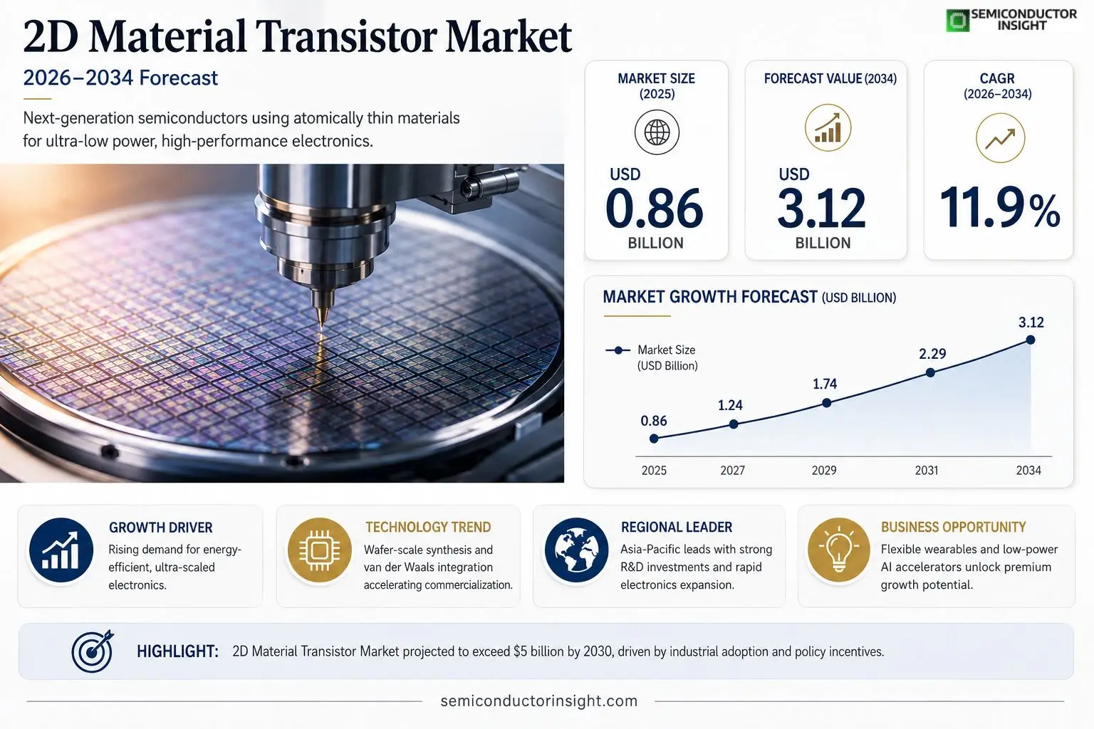
Global 2D Material Transistor Market size was valued at USD 0.86 billion in 2025. The market is projected to grow from USD 0.86 billion in 2025 to USD 3.12 billion by 2034, exhibiting a CAGR of 11.9% during the forecast period.
2D material transistors are semiconductor devices that utilize atomically thin layers,such as graphene, molybdenum disulfide (MoS₂), tungsten diselenide (WSe₂), and black phosphorus,to achieve superior electro‑static control, high carrier mobility, and flexible form factors. These characteristics enable ultra‑scaled logic gates, high‑frequency RF components, and emerging flexible electronics.The market is experiencing rapid growth because substantial R&D investments from leading fabs and technology firms are accelerating commercialization of wafer‑scale synthesis techniques. However, challenges related to large‑area uniformity and reliable contact engineering persist. Furthermore, rising demand for low‑power AI accelerators and next‑generation mobile processors fuels adoption of 2D material transistors. Key players such as Samsung Electronics, Intel Corporation, IBM Research, TSMC, and GlobalFoundries are actively forming partnerships and launching pilot production lines to capture early market share.
MARKET DRIVERS
Rising Demand for Energy‑Efficient Electronics
The global push toward lower power consumption in smartphones, data‑center processors, and IoT devices is accelerating adoption of ultra‑thin, low‑loss semiconductors. 2D Material Transistor Market participants are capitalizing on the ability of graphene and transition‑metal dichalcogenides to deliver sub‑10 nm channel lengths while maintaining high carrier mobility.
Advancements in Van der Waals Heterostructure Integration
Recent breakthroughs in deterministic stacking of atomically thin layers enable seamless integration of complementary logic circuits. This technical progress reduces interface defects and positions 2D Material Transistor Market as a viable alternative to traditional silicon CMOS for next‑generation processors.
➤ 2D Material Transistor Market is projected to exceed $5 billion by 2030, driven by expanded industrial adoption and policy incentives for sustainable electronics.
Strategic partnerships between semiconductor manufacturers and research institutions are translating laboratory concepts into volume‑ready production lines, further reinforcing market momentum.
MARKET CHALLENGES
Manufacturing Scalability Constraints
Scaling up wafer‑scale synthesis of high‑quality monolayers remains costly, and variability in layer uniformity hampers yield. These factors increase capital expenditures for early adopters and slow broader market penetration.
Other Challenges
Yield Variability
Inconsistent defect densities across large‑area films lead to performance fluctuations, forcing manufacturers to implement rigorous inspection regimes that add to production overhead.
MARKET RESTRAINTS
High Material Synthesis Costs
Current chemical vapor deposition and molecular beam epitaxy processes require specialized equipment and high‑purity precursors, resulting in unit costs that are markedly higher than conventional silicon wafers. This cost premium restricts adoption to high‑value segments such as aerospace and advanced computing.
MARKET OPPORTUNITIES
Emerging Applications in Flexible Wearables
Wearable health monitors and smart textiles demand transistors that retain performance under mechanical strain. The inherent flexibility of 2‑D crystals opens a niche where 2D Material Transistor Market can command premium pricing, especially as consumer demand for discreet, high‑performance sensors grows.
2D Material Transistor Market Trends
Rapid Commercialization of Wafer‑Scale Synthesis
2D Material Transistor Market is experiencing a decisive shift as semiconductor giants allocate substantial R&D budgets toward wafer‑scale production of atomically thin semiconductors such as graphene, molybdenum disulfide (MoS₂) and tungsten diselenide (WSe₂). By scaling the synthesis process, manufacturers can achieve consistent film thickness across 300‑mm wafers, which directly reduces material waste and improves device yield. This manufacturing maturity is unlocking new design opportunities for ultra‑low‑power AI accelerators, high‑frequency RF modules, and flexible display back‑planes. The convergence of cost‑effective large‑area growth and mature lithography enables designers to replace traditional silicon channels with 2D alternatives, offering superior electro‑static control and higher carrier mobility while maintaining compatibility with existing CMOS fabs.
Other Trends
Process Uniformity and Contact Engineering
Achieving uniformity across the entire wafer remains a critical challenge for 2D Material Transistor Market. Small variations in layer thickness or defect density can cause significant performance spread, impacting overall chip reliability. To mitigate these effects, manufacturers are adopting plasma‑treated substrate preparations and in‑situ cleaning steps that promote nucleation uniformity. Concurrently, contact resistance is being lowered through edge‑contact configurations and the introduction of two‑dimensional metallic interlayers, which provide more stable Schottky barriers. These technical advances are gradually narrowing the gap between laboratory‑scale demonstrations and high‑volume production, fostering greater confidence among design houses and end‑users.
Strategic Partnerships and Ecosystem Development
Major industry players,including Samsung Electronics, Intel Corporation, IBM Research, TSMC, and GlobalFoundries,are forging strategic alliances with specialized material suppliers and academic consortia. These partnerships accelerate the transfer of breakthrough synthesis techniques into fab‑ready processes, while joint development programs standardize design‑automation libraries for 2D devices. By establishing a collaborative ecosystem, 2D Material Transistor Market benefits from shared risk, faster qualification cycles, and a growing pool of qualified engineers. The resulting momentum is evident in an increasing number of pilot production lines that integrate 2D channel transistors into low‑power logic blocks and flexible sensor arrays, signaling a clear pathway toward broader commercial adoption.
COMPETITIVE LANDSCAPEKey Industry Players
2D Material Transistor Market Competitive Landscape
2D Material Transistor Market is anchored by a handful of semiconductor giants that are leveraging large‑scale wafer fabrication capabilities to transition from pilot lines to volume production. Samsung Electronics leads the race by integrating graphene and MoS₂ channels into its advanced logic nodes, supported by multi‑billion‑dollar R&D spend and a global foundry network. Intel Corporation follows with a dedicated 2D‑materials research consortium aimed at low‑power AI accelerators, while IBM Research continues to publish breakthrough contact‑engineering studies that reduce resistance in ultra‑thin channels. Taiwanese Semiconductor Manufacturing Company (TSMC) and GlobalFoundries have both announced joint ventures with academic partners to secure wafer‑scale synthesis, positioning them as critical enablers of supply chain reliability. Collectively, these incumbents shape market structure through strategic alliances, IP licensing, and early‑stage pilot production that set performance benchmarks for the emerging ecosystem.Beyond the largest fabs, a vibrant cohort of specialized firms and university spin‑offs fuels innovation in niche applications and equipment supply. Graphene Square, a European startup, focuses on flexible display transistors using chemically vapor‑deposited graphene. Nanjing University’s “Jiangsu 2D Materials” spin‑off supplies high‑uniformity MoS₂ wafers for RF components, while CVD Equipment Inc. provides custom deposition tools critical for scaling to 150 mm substrates. Sony Corporation is experimenting with black‑phosphorus channels for high‑frequency imaging sensors, and STMicroelectronics has introduced a prototype mixed‑signal chip that integrates 2D channels with legacy CMOS. These players, though smaller in revenue, contribute essential process know‑how, niche device architectures, and a pipeline of applications that broaden the market’s reach and foster competition.
List of Key 2D Material Transistor Companies Profiled
- Samsung Electronics
- Intel Corporation
- IBM Research
- TSMC
- GlobalFoundries
- Jiangsu 2D Materials (Nanjing University spin‑off)
- Graphene Square
- CVD Equipment Inc.
- 2D Transistor Ltd. (NTU spin‑off)
- Sony Corporation
- STMicroelectronics
- Applied Materials
Segment Analysis:
| Segment Category | Sub-Segments | Key Insights |
| By Type |
|
Graphene transistors are favored for ultra‑high carrier mobility and excellent thermal conductivity.
|
| By Application |
|
Logic gates drive the core of emerging low‑power AI accelerators and mobile CPUs.
|
| By End User |
|
Semiconductor manufacturers are actively piloting wafer‑scale 2D synthesis to secure early‑stage supply.
|
| By Device Architecture |
|
Planar 2D transistors remain the leading architecture for early adoption.
|
| By Performance Requirement |
|
Low‑power devices drive the primary demand from AI edge and mobile markets.
|
Regional Analysis: North America
North America
Significant investments in academic and industrial R&D are fostering breakthroughs in 2D material synthesis and transistor fabrication techniques. This drive towards innovation is crucial for overcoming existing challenges and unlocking the full potential of 2D material transistors.
The increasing demand for flexible displays, wearable electronics, and high-frequency communication systems is creating substantial opportunities for 2D material transistors to replace conventional silicon-based transistors.
North America boasts a dynamic competitive landscape with established semiconductor companies and emerging startups vying for market share. Strategic partnerships and collaborations are becoming increasingly important for navigating this competitive environment.
Government initiatives and funding programs play a vital role in supporting the development and commercialization of 2D material transistor technology in North America. These efforts are instrumental in fostering innovation and attracting private investment.
Europe
Europe presents a steadily growing market for 2D Material Transistor Market. Strong emphasis on sustainable technologies and advanced manufacturing processes is driving adoption. The region’s robust industrial base and collaborative research environment are conducive to innovation in this field. Key areas of focus include energy-efficient electronics and advanced sensor technologies. European initiatives promoting technological advancement are further bolstering the market’s prospects.
Asia-Pacific
Asia-Pacific is expected to witness the fastest growth in 2D Material Transistor Market. The region’s burgeoning electronics industry, particularly in China and South Korea, is a primary driver. Increasing investments in research and development, coupled with supportive government policies, are fueling market expansion. Applications in flexible displays, IoT devices, and advanced computing are creating significant demand.
South America
South America is an emerging market for 2D Material Transistor Market, with potential for growth in the coming years. The increasing adoption of smartphones, tablets, and other electronic devices is driving demand. Investments in technology and infrastructure are expected to further stimulate market expansion. The focus is on cost-effective solutions and applications in consumer electronics and industrial sensors.
Middle East & Africa
The Middle East & Africa represents a relatively nascent market for 2D Material Transistor Market. However, increasing investments in technological advancements and infrastructure development are creating opportunities. The growing demand for smart devices and industrial automation is expected to drive market growth in the region. The focus is on sectors like energy, healthcare, and telecommunications.
Report Scope
This market research report provides a comprehensive analysis of the 2D Material Transistor Market , covering the forecast period 2026–2034. It offers detailed insights into market dynamics, technological advancements, competitive landscape, and key trends shaping the industry.
Key focus areas of the report include:
- ✅ Market Overview: The report begins with an overview outlining its current market scenario, key growth indicators, and industry transformation drivers. It discusses macroeconomic factors, demand–supply balance, regulatory landscape, and the strategic role of semiconductors in powering advancements across industries such as automotive, telecommunications, consumer electronics, and industrial automation.
- ✅ Market Size & Forecast: Historical data and future projections for revenue, unit shipments, and market value across major regions and segments.
- ✅ Segmentation Analysis: Detailed breakdown by product type, technology, application, and end-user industry to identify high-growth segments and investment opportunities.
- ✅ Regional Insights: Insights into market performance across North America, Europe, Asia-Pacific, Latin America, and the Middle East & Africa, including country-level analysis where relevant.
- ✅ Competitive Landscape: Profiles of leading market participants, including their product offerings, R&D focus, manufacturing capacity, pricing strategies, and recent developments such as mergers, acquisitions, and partnerships.
- ✅ Technology Trends & Innovation: Assessment of emerging technologies, integration of AI/IoT, semiconductor design trends, fabrication techniques, and evolving industry standards.
- ✅ Market Drivers & Restraints: Evaluation of factors driving market growth along with challenges, supply chain constraints, regulatory issues, and market-entry barriers.
- ✅ Stakeholder Insights: Insights for component suppliers, OEMs, system integrators, investors, and policymakers regarding the evolving ecosystem and strategic opportunities.
Primary and secondary research methods are employed, including interviews with industry experts, data from verified sources, and real-time market intelligence to ensure the accuracy and reliability of the insights presented.
FREQUENTLY ASKED QUESTIONS:
What is the current market size of 2D Material Transistor Market?
-> 2D Material Transistor Market was valued at USD 0.86 billion in 2025 and is expected to reach USD 3.12 billion by 2034, exhibiting a CAGR of 11.9% during the forecast period.
Which key companies operate in 2D Material Transistor Market?
-> Key players include Samsung Electronics, Intel Corporation, IBM Research, TSMC, GlobalFoundries, among others.
What are the key growth drivers?
-> Key growth drivers include substantial R&D investments, commercialization of wafer‑scale synthesis techniques, rising demand for low‑power AI accelerators, and next‑generation mobile processors.
Which region dominates the market?
-> North America and Asia‑Pacific are the leading regions driving market growth, while Europe also holds a strong presence.
What are the emerging trends?
-> Emerging trends include advancements in wafer‑scale synthesis, integration with AI/IoT platforms, and the development of flexible and low‑power 2D transistor architectures.

Get Sample Report PDF for Exclusive Insights
Report Sample Includes
- Table of Contents
- List of Tables & Figures
- Charts, Research Methodology, and more...