
2D Material Semiconductor Market Insights
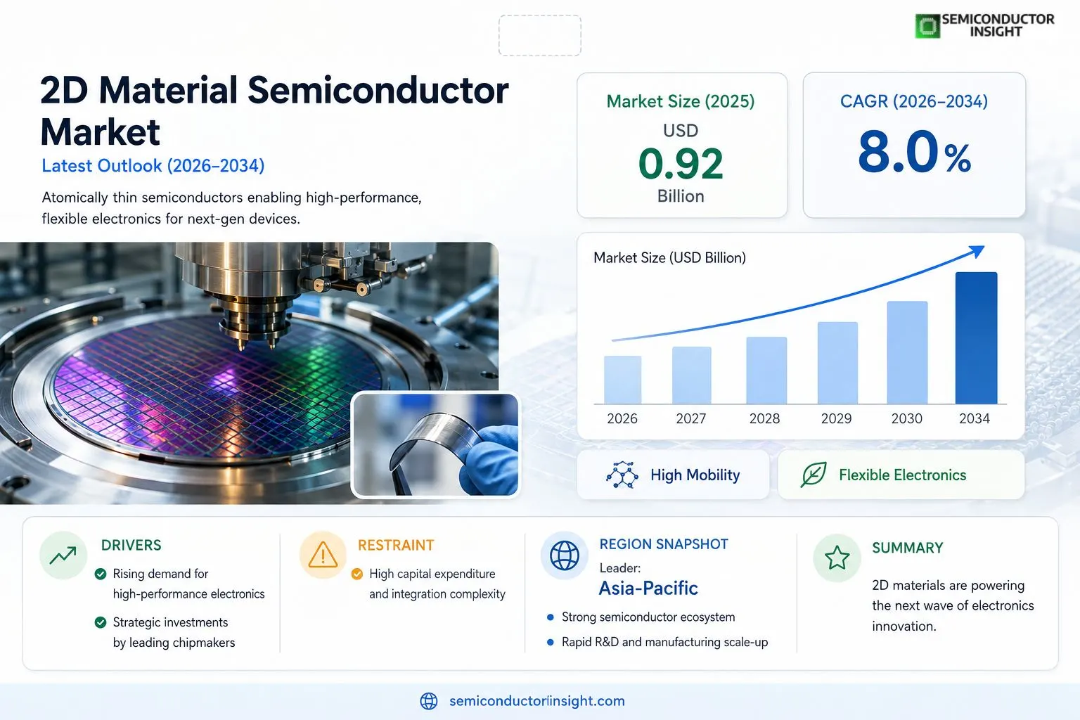
Global 2D material semiconductor market size was valued at USD 0.92 billion in 2025. The market is projected to grow from USD 0.92 billion in 2025 to USD 1.84 billion by 2034, exhibiting a CAGR of 8.0% during the forecast period.
2D material semiconductors refer to atomically thin crystalline layers,such as graphene, transition‑metal dichalcogenides (e.g., MoS₂, WS₂), phosphorene and hexagonal boron nitride,engineered to function as active electronic components. Their unique band‑gap tunability, high carrier mobility and mechanical flexibility enable applications ranging from ultra‑thin transistors and flexible displays to photodetectors and quantum‑computing interfaces.The market is experiencing rapid growth due to several factors, including escalating R&D investments from leading chipmakers, rising demand for high‑performance low‑power devices in consumer electronics, and expanding adoption of flexible and wearable technologies. Furthermore, breakthroughs in large‑area synthesis techniques,such as chemical vapor deposition (CVD) scaling,and strategic collaborations among semiconductor giants like Samsung Electronics, Intel Corporation, Taiwan Semiconductor Manufacturing Company (TSMC) and research consortia accelerate commercialization pathways.
MARKET DRIVERS
Rising Demand for High‑Performance Electronics
2D Material Semiconductor Market is being propelled by the rapid expansion of high‑performance computing devices, where traditional silicon faces physical limitations. Engineers are turning to atomically thin materials such as graphene and transition‑metal dichalcogenides to achieve superior carrier mobility and lower power consumption. This shift is creating a strong growth catalyst for manufacturers that can integrate 2‑D layers into existing fab lines.
Strategic Investments by Leading Chipmakers
Major semiconductor players have announced multi‑billion‑dollar R&D programs focused on 2‑D material integration, accelerating technology readiness. These investments are coupled with government incentives for advanced materials, fostering an innovation ecosystem that shortens time‑to‑market for novel devices. As a result, the overall market outlook is becoming increasingly bullish.
➤ “The convergence of flexible electronics and 2‑D semiconductors is expected to unlock new product categories worth over $10 billion by 2030.”
Finally, the push for miniaturization in IoT sensors and wearable health monitors is driving designers to adopt 2‑D materials for their ultra‑thin form factor, further expanding the addressable market for 2D Material Semiconductor Market.
MARKET CHALLENGES
Manufacturing Yield and Process Integration
Current fabrication techniques for 2‑D layers often suffer from low yield and inconsistent film quality, which hampers large‑scale adoption. The need to align atomically thin sheets with existing silicon wafers introduces process complexity that can increase production costs and delay time‑to‑revenue.
Other Challenges
Supply Chain Complexity
The sourcing of high‑purity precursor materials remains limited to a few specialized suppliers. Any disruption can create bottlenecks, making it difficult for manufacturers to scale operations reliably across global markets.
MARKET RESTRAINTS
High Capital Expenditure
Establishing dedicated 2‑D material fabrication lines requires substantial upfront investment in equipment such as atomic‑layer deposition and transfer printing systems. For many midsize enterprises, the financial barrier remains a decisive restraint.Additionally, the lack of standardized testing protocols for 2‑D semiconductor performance creates uncertainty in product qualification, limiting confidence among downstream adopters.
MARKET OPPORTUNITIES
Emerging Applications in Quantum Devices
The unique electronic properties of 2‑D materials, such as tunable bandgaps and strong spin‑orbit coupling, open pathways for quantum computing and ultra‑secure communication systems. Early‑stage collaborations between academia and industry are positioning 2D Material Semiconductor Market to capture significant value as these technologies mature.Furthermore, the growing demand for flexible and transparent displays presents a sizable opportunity for 2‑D semiconductors, where their mechanical robustness and optical clarity can replace conventional thin‑film transistors in next‑generation consumer electronics.
2D Material Semiconductor Market Trends
Growth Driven by R&D Investment
2D Material Semiconductor Market is experiencing accelerated adoption as leading chip manufacturers increase research budgets for atomically thin channels. Recent breakthroughs in graphene and transition‑metal dichalcogenide processing have reduced defect density, enabling high‑performance low‑power transistors for next‑generation smartphones and edge‑AI modules. Coupled with rising consumer demand for flexible displays and wearable sensors, the market trajectory reflects a shift from laboratory prototypes to volume production. Strategic alliances between semiconductor giants and materials specialists further streamline supply chains, shortening time‑to‑market for novel device architectures. Environmental regulations also favor low‑temperature processes, as 2D material deposition typically consumes less energy than bulk semiconductor growth. Moreover, government initiatives in Europe and Asia provide subsidies for thin‑film research, reinforcing the investment pipeline. Integrated device demonstrations now show multi‑layer heterostructures that combine graphene’s conductivity with MoS₂’s semiconducting properties, unlocking new circuit functionalities such as on‑chip optoelectronic switches. These developments collectively reinforce the upward trajectory of the market.
Other Trends
Large‑Area Synthesis Advances
Large‑area synthesis techniques have moved from small‑flake exfoliation to scalable chemical vapor deposition (CVD) processes that cover entire 300‑mm wafers. Recent pilot lines demonstrate uniform layer thickness and controllable doping across wafer‑scale substrates, meeting the stringent uniformity requirements of modern logic fabs. Collaborative programs between TSMC, Intel and leading research institutes accelerate technology transfer, allowing foundries to integrate 2D channels alongside conventional silicon without major equipment overhauls. These advances lower production costs and improve yield, positioning the market for broader commercial uptake. In addition, advanced in‑situ metrology using Raman spectroscopy and ellipsometry provides real‑time feedback, enabling precise control of layer thickness and strain. Yield optimization efforts focus on reducing contamination during transfer processes, which historically limited large‑scale adoption. By integrating these monitoring techniques into production lines, manufacturers achieve defect densities below 10⁹ cm⁻², aligning with the reliability standards of advanced logic nodes.
Application Expansion in Wearables
Application diversification continues to drive momentum, with flexible wearable electronics, photonic sensors, and quantum‑interface components emerging as high‑growth segments. Device designers exploit the tunable band‑gap of transition‑metal dichalcogenides to create wavelength‑selective photodetectors, while graphene’s exceptional conductivity supports ultra‑fast interconnects in emerging neuromorphic chips. As standards evolve and design‑tool ecosystems mature, 2D Material Semiconductor Market is set to mature into a foundational technology layer for next‑generation computing and communications platforms. Supply chain resilience is also improving, as vertical integration strategies allow chipmakers to source high‑purity precursors and custom‑grown substrates directly from materials firms. This reduces dependence on third‑party vendors and shortens lead times for prototype iterations. As the ecosystem matures, industry standards for interface characterization and reliability testing are expected to converge, further de‑risking large‑scale deployment. Consequently, 2D Material Semiconductor Market is poised to transition from niche high‑performance applications toward mainstream integration across consumer, automotive, and aerospace sectors.
COMPETITIVE LANDSCAPEKey Industry Players
Competitive Dynamics in 2D Material Semiconductor Market
2D Material Semiconductor Market is currently dominated by a handful of integrated‑device powerhouses that have leveraged extensive R&D budgets and advanced manufacturing ecosystems to transition atomically thin channels from laboratory to fab. Samsung Electronics leads the segment, capitalising on its CD‑based graphene‑on‑silicon prototypes and its partnership with academic consortia to scale CVD growth. Intel Corporation follows closely, integrating MoS₂ and WS₂ channels into its low‑power logic roadmap, while Taiwan Semiconductor Manufacturing Company (TSMC) provides the high‑volume foundry services that enable multi‑layer heterostructure stacks for clients. These three firms shape the market’s top‑down structure, dictating supply‑chain standards, device architectures, and price points for downstream OEMs.Beyond the tier‑one fabs, a vibrant ecosystem of specialised players advances niche applications and supplies critical IP. The Graphene Flagship consortium and its industrial partners such as Graphenea and Haydale drive large‑area graphene synthesis for flexible displays and sensor arrays. Nantero and XG Sciences focus on graphene‑based nanoribbon transistors targeting ultra‑high‑frequency communications. Applied Materials offers CVD and ALD equipment that underpins mass production of transition‑metal dichalcogenides. Start‑ups like 2D Semiconductor (now part of AXT) and Talga Technologies commercialise wafer‑scale MoS₂ for photodetectors and quantum‑bits. Second Quantum supplies high‑purity h‑BN substrates for quantum‑computing interfaces. Collectively, these niche innovators diversify the supply base, accelerate technology validation, and create interchangeable pathways for customers seeking performance beyond conventional silicon.
List of Key 2D Material Semiconductor Companies Profiled
- Samsung Electronics
- Intel Corporation
- Taiwan Semiconductor Manufacturing Company (TSMC)
- Graphene Flagship Consortium
- Haydale Graphene Industries
- Nantero Inc.
- XG Sciences
- Applied Materials
- 2D Semiconductor (AXT)
- Talga Technologies
- Second Quantum
- Cambridge Nanosystems
- Avant Materials
Segment Analysis:
| Segment Category | Sub-Segments | Key Insights |
| By Type |
|
Graphene‑based Semiconductors are emerging as the leading sub‑segment due to their exceptional carrier mobility and flexibility.
|
| By Application |
|
Flexible Displays dominate the application landscape, driven by the need for lightweight, bendable screens.
|
| By End User |
|
Consumer Electronics Manufacturers are the primary drivers, embracing 2D materials to deliver next‑generation smartphones and tablets.
|
| By Technology |
|
CVD Scale‑up Techniques are pivotal, unlocking large‑area synthesis for commercial volume.
|
| By Market Adoption |
|
Pilot‑Scale Production represents the most active phase, where collaborative ecosystems validate manufacturability.
|
Regional Analysis: North America
United States
The United States boasts a strong foundation in materials science, with numerous research labs and universities actively engaged in exploring new 2D material synthesis and characterization techniques. This focus on fundamental research is crucial for driving future technological breakthroughs in 2D Material Semiconductor Market.
Strategic collaborations between academic institutions, government agencies, and private companies are fostering innovation and accelerating the commercialization of 2D material semiconductor technologies in the US. These partnerships are vital for bridging the gap between research and practical applications.
Significant venture capital and government funding are being directed towards 2D material semiconductor startups and research projects in the United States, indicating a strong belief in the long-term potential of these materials. This financial support is crucial for scaling up production and driving market adoption.
Efforts are underway to develop robust and sustainable supply chains for key 2D materials in the US, addressing potential bottlenecks and ensuring a reliable source of these critical components for the semiconductor industry.
Europe
Europe is witnessing increasing interest in 2D Material Semiconductor Market, with several countries actively investing in research and development initiatives. The region’s strong emphasis on sustainable technologies and advanced manufacturing is driving demand for these materials. Key players are focusing on applications in flexible electronics, sensors, and energy-efficient devices. Government funding programs across Europe are supporting collaborative projects aimed at accelerating the translation of 2D material research into commercial products. The European Union’s initiatives promoting technological sovereignty further bolster the market’s potential. While the pace of adoption may be slightly slower compared to the US, Europe is poised for significant growth in the coming years, particularly in niche applications where its technological strengths align with 2D material capabilities. 2D Material Semiconductor Market in Europe is showing steady expansion.
Asia-Pacific
Asia-Pacific represents a dynamic and rapidly expanding market for 2D material semiconductors. Countries like China, Japan, and South Korea are leading the charge, driven by strong domestic semiconductor industries and supportive government policies. The region’s dominance in manufacturing and electronics production fuels significant demand for these advanced materials. Focus areas include applications in high-performance computing, foldable displays, and advanced sensors. Extensive investments in R&D and the development of large-scale production facilities are further accelerating market growth. The Asia-Pacific region’s competitive landscape is characterized by a mix of established players and emerging startups, creating a vibrant ecosystem for innovation. 2D Material Semiconductor Market in Asia-Pacific is experiencing exponential growth.
South America
2D Material Semiconductor Market in South America is in its nascent stages but is beginning to attract attention. Countries like Brazil and Argentina are exploring potential applications in areas such as flexible electronics and sensors for industrial and consumer use. Limited R&D infrastructure and smaller market size pose challenges, but growing investments in technology and a rising demand for advanced electronic devices are creating opportunities. The region’s focus on resource utilization could also drive interest in 2D materials for energy-related applications. 2D Material Semiconductor Market in South America presents long-term growth potential.
Middle East & Africa
2D Material Semiconductor Market in the Middle East and Africa is a developing area with significant growth potential. Countries in this region are increasingly focused on diversifying their economies and investing in technology. Applications in sensors for industrial monitoring, energy management, and emerging communication technologies are expected to drive demand. Government initiatives promoting technological advancement and a growing electronics sector are contributing to the market’s expansion. While the market is currently small, the region’s long-term growth trajectory suggests a promising outlook for 2D material semiconductors. 2D Material Semiconductor Market in Middle East & Africa is poised for considerable expansion.
Report Scope
This market research report provides a comprehensive analysis of the 2D Material Semiconductor Market , covering the forecast period 2026–2034. It offers detailed insights into market dynamics, technological advancements, competitive landscape, and key trends shaping the industry.
Key focus areas of the report include:
- Market Overview: The report begins with an overview outlining its current market scenario, key growth indicators, and industry transformation drivers. It discusses macroeconomic factors, demand–supply balance, regulatory landscape, and the strategic role of semiconductors in powering advancements across industries such as automotive, telecommunications, consumer electronics, and industrial automation.
- Market Size & Forecast: Historical data and future projections for revenue, unit shipments, and market value across major regions and segments.
- Segmentation Analysis: Detailed breakdown by product type, technology, application, and end-user industry to identify high-growth segments and investment opportunities.
- Regional Insights: Insights into market performance across North America, Europe, Asia-Pacific, Latin America, and the Middle East & Africa, including country-level analysis where relevant.
- Competitive Landscape: Profiles of leading market participants, including their product offerings, R&D focus, manufacturing capacity, pricing strategies, and recent developments such as mergers, acquisitions, and partnerships.
- Technology Trends & Innovation: Assessment of emerging technologies, integration of AI/IoT, semiconductor design trends, fabrication techniques, and evolving industry standards.
- Market Drivers & Restraints: Evaluation of factors driving market growth along with challenges, supply chain constraints, regulatory issues, and market-entry barriers.
- Stakeholder Insights: Insights for component suppliers, OEMs, system integrators, investors, and policymakers regarding the evolving ecosystem and strategic opportunities.
Primary and secondary research methods are employed, including interviews with industry experts, data from verified sources, and real-time market intelligence to ensure the accuracy and reliability of the insights presented.
FREQUENTLY ASKED QUESTIONS:
What is the current market size of 2D Material Semiconductor Market?
-> 2D Material Semiconductor Market was valued at USD 0.92 billion in 2025 and is expected to reach USD 1.84 billion by 2034.
Which key companies operate in 2D Material Semiconductor Market?
-> Key players include Samsung Electronics, Intel Corporation, Taiwan Semiconductor Manufacturing Company (TSMC), IBM, and leading research institutions such as the University of Manchester, among others.
What are the key growth drivers?
-> Key growth drivers include escalating R&D investments from leading chipmakers, rising demand for high‑performance low‑power devices in consumer electronics, and expanding adoption of flexible and wearable technologies.
Which region dominates the market?
-> Asia‑Pacific is the fastest‑growing region, while North America remains a dominant market.
What are the emerging trends?
-> Emerging trends include large‑area chemical vapor deposition (CVD) scaling, heterostructure integration, and development of quantum‑computing interfaces.

Get Sample Report PDF for Exclusive Insights
Report Sample Includes
- Table of Contents
- List of Tables & Figures
- Charts, Research Methodology, and more...
 Download Sample Report PDF


