200mm Wafers Market Overview
This report studies the 8-inch or 200mm Silicon Wafer market. Semiconductor silicon wafers are key component of integrated circuits such as those used to power computers, cell phones, and a wide variety of other devices. A silicon wafer consists of a thin slice of silicon which can be treated in various ways, depending on the type of electronics that is being used. Silicon has a very high quality semiconductor, making it ideal for the production of such circuits.
This report provides a deep insight into the global 200mm Wafers market covering all its essential aspects. This ranges from a macro overview of the market to micro details of the market size, competitive landscape, development trend, niche market, key market drivers and challenges, SWOT analysis, value chain analysis, etc.
The analysis helps the reader to shape the competition within the industries and strategies for the competitive environment to enhance the potential profit. Furthermore, it provides a simple framework for evaluating and accessing the position of the business organization. The report structure also focuses on the competitive landscape of the Global 200mm Wafers Market, this report introduces in detail the market share, market performance, product situation, operation situation, etc. of the main players, which helps the readers in the industry to identify the main competitors and deeply understand the competition pattern of the market.
In a word, this report is a must-read for industry players, investors, researchers, consultants, business strategists, and all those who have any kind of stake or are planning to foray into the 200mm Wafers market in any manner.
200mm Wafers Market Analysis:
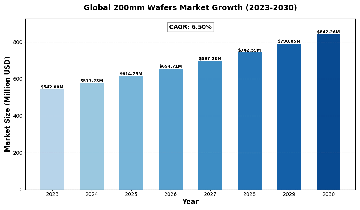
The global 200mm Wafers market size was estimated at USD 542 million in 2023 and is projected to reach USD 842.26 million by 2030, exhibiting a CAGR of 6.50% during the forecast period.
North America 200mm Wafers market size was USD 141.23 million in 2023, at a CAGR of 5.57% during the forecast period of 2025 through 2030.
200mm Wafers Key Market Trends :
Rising Demand for Power and Analog Semiconductors
The increasing need for power management and analog devices in automotive, industrial, and IoT applications is driving demand for 200mm wafers.Expansion of 200mm Fab Capacities
Semiconductor manufacturers are expanding their 200mm wafer production facilities to meet the growing demand, especially for legacy node applications.Shift Towards 5G and Automotive Electronics
The expansion of 5G networks and the rise of electric vehicles are boosting the adoption of 200mm wafers for power and RF semiconductor applications.Increase in Foundry Investments
Major foundries are investing in 200mm wafer production to support growing customer demand for cost-effective semiconductor solutions.Supply Chain Optimization for Semiconductor Manufacturing
Companies are focusing on improving supply chain efficiency and securing raw materials to ensure uninterrupted 200mm wafer production.
200mm Wafers Market Regional Analysis :

- North America:Strong demand driven by EVs, 5G infrastructure, and renewable energy, with the U.S. leading the market.
- Europe:Growth fueled by automotive electrification, renewable energy, and strong regulatory support, with Germany as a key player.
- Asia-Pacific:Dominates the market due to large-scale manufacturing in China and Japan, with growing demand from EVs, 5G, and semiconductors.
- South America:Emerging market, driven by renewable energy and EV adoption, with Brazil leading growth.
- Middle East & Africa:Gradual growth, mainly due to investments in renewable energy and EV infrastructure, with Saudi Arabia and UAE as key contributors.
200mm Wafers Market Segmentation
The research report includes specific segments by region (country), manufacturers, Type, and Application. Market segmentation creates subsets of a market based on product type, end-user or application, Geographic, and other factors. By understanding the market segments, the decision-maker can leverage this targeting in the product, sales, and marketing strategies. Market segments can power your product development cycles by informing how you create product offerings for different segments.
Key Company
- Shin-Etsu Chemical
- Sumco
- Global Wafers
- Siltronic
- SK siltron
- Waferworks
- Ferrotec
- AST
- Gritek
- Guosheng
- QL Electronics
- MCL
- National Silicon Industry Group
- Poshing
Market Segmentation (by Type)
- Polished Wafer
- Epitaxial Wafer
- Annealed Wafer
- Others
Market Segmentation (by Application)
- Memory
- Logic/MPU
- Analog
- Discrete Device and Sensor
- Others
Drivers
Growing Demand for Consumer Electronics
The rise in smartphones, wearables, and smart home devices is increasing the need for 200mm wafers in semiconductor production.Expansion of Automotive Semiconductor Applications
The automotive industry is adopting 200mm wafers for power electronics, sensors, and logic devices in electric and autonomous vehicles.Cost-Effective Manufacturing for Legacy Nodes
200mm wafers remain a cost-efficient solution for manufacturing legacy semiconductor nodes, making them a preferred choice for foundries.
Restraints
Limited Availability of 200mm Equipment
The supply of 200mm wafer fabrication tools is constrained as manufacturers focus on newer 300mm technologies, creating a bottleneck for expansion.Fluctuating Raw Material Prices
The volatility in silicon prices and supply chain disruptions can impact the cost and availability of 200mm wafers.Increasing Competition from 300mm Wafers
The transition towards 300mm wafers for advanced semiconductor applications is posing a challenge to the growth of the 200mm wafer market.
Opportunities
Rising Demand for IoT and Industrial Applications
The growing adoption of IoT devices and industrial automation is creating new opportunities for 200mm wafers in sensor and analog device production.Investment in 200mm Wafer Fabs
Semiconductor companies and governments are investing in 200mm wafer fabrication plants to strengthen supply chains and meet increasing demand.Advancements in Wafer Processing Technologies
Innovations in wafer thinning, polishing, and epitaxial growth are enhancing the performance and reliability of 200mm wafers for various applications.
Challenges
Supply Chain Disruptions in Semiconductor Manufacturing
Global supply chain constraints and geopolitical tensions are affecting the availability of raw materials and manufacturing equipment.Capacity Constraints at Foundries
The high demand for 200mm wafers is exceeding production capacity at existing foundries, leading to longer lead times and potential shortages.Technological Limitations Compared to Advanced Nodes
While 200mm wafers are essential for legacy semiconductor nodes, they face limitations in supporting high-performance computing and AI-driven applications.
Key Benefits of This Market Research:
- Industry drivers, restraints, and opportunities covered in the study
- Neutral perspective on the market performance
- Recent industry trends and developments
- Competitive landscape & strategies of key players
- Potential & niche segments and regions exhibiting promising growth covered
- Historical, current, and projected market size, in terms of value
- In-depth analysis of the CMP Consumable Parts Market
- Overview of the regional outlook of the CMP Consumable Parts Market:
Key Reasons to Buy this Report:
- Access to date statistics compiled by our researchers. These provide you with historical and forecast data, which is analyzed to tell you why your market is set to change
- This enables you to anticipate market changes to remain ahead of your competitors
- You will be able to copy data from the Excel spreadsheet straight into your marketing plans, business presentations, or other strategic documents
- The concise analysis, clear graph, and table format will enable you to pinpoint the information you require quickly
- Provision of market value data for each segment and sub-segment
- Indicates the region and segment that is expected to witness the fastest growth as well as to dominate the market
- Provides insight into the market through Value Chain
- Market dynamics scenario, along with growth opportunities of the market in the years to come
- 6-month post-sales analyst support
Customization of the Report
In case of any queries or customization requirements, please connect with our sales team, who will ensure that your requirements are met.
FAQs
What are the key driving factors and opportunities in the 200mm Wafers market?
The key drivers include rising demand for analog and power semiconductors, increasing automotive semiconductor adoption, and cost-effective manufacturing for legacy nodes. Opportunities lie in IoT applications, expanding 200mm fab investments, and advancements in wafer processing technologies.
Which region is projected to have the largest market share?
Asia-Pacific is expected to dominate the 200mm wafers market, driven by strong semiconductor manufacturing activity in China, Taiwan, South Korea, and Japan.
Who are the top players in the global 200mm Wafers market?
Leading companies include Shin-Etsu Chemical, Sumco, Global Wafers, Siltronic, SK Siltron, Waferworks, Ferrotec, and AST.
What are the latest technological advancements in the industry?
Key advancements include improved wafer thinning techniques, epitaxial wafer enhancements, and automation in 200mm wafer production to increase yield and efficiency.
What is the current size of the global 200mm Wafers market?
The market was valued at USD 542 million in 2023 and is projected to reach USD 842.26 million by 2030, growing at a CAGR of 6.50% during the forecast period.

Get Sample Report PDF for Exclusive Insights
Report Sample Includes
- Table of Contents
- List of Tables & Figures
- Charts, Research Methodology, and more...