Photomask Inspection System Market Insights
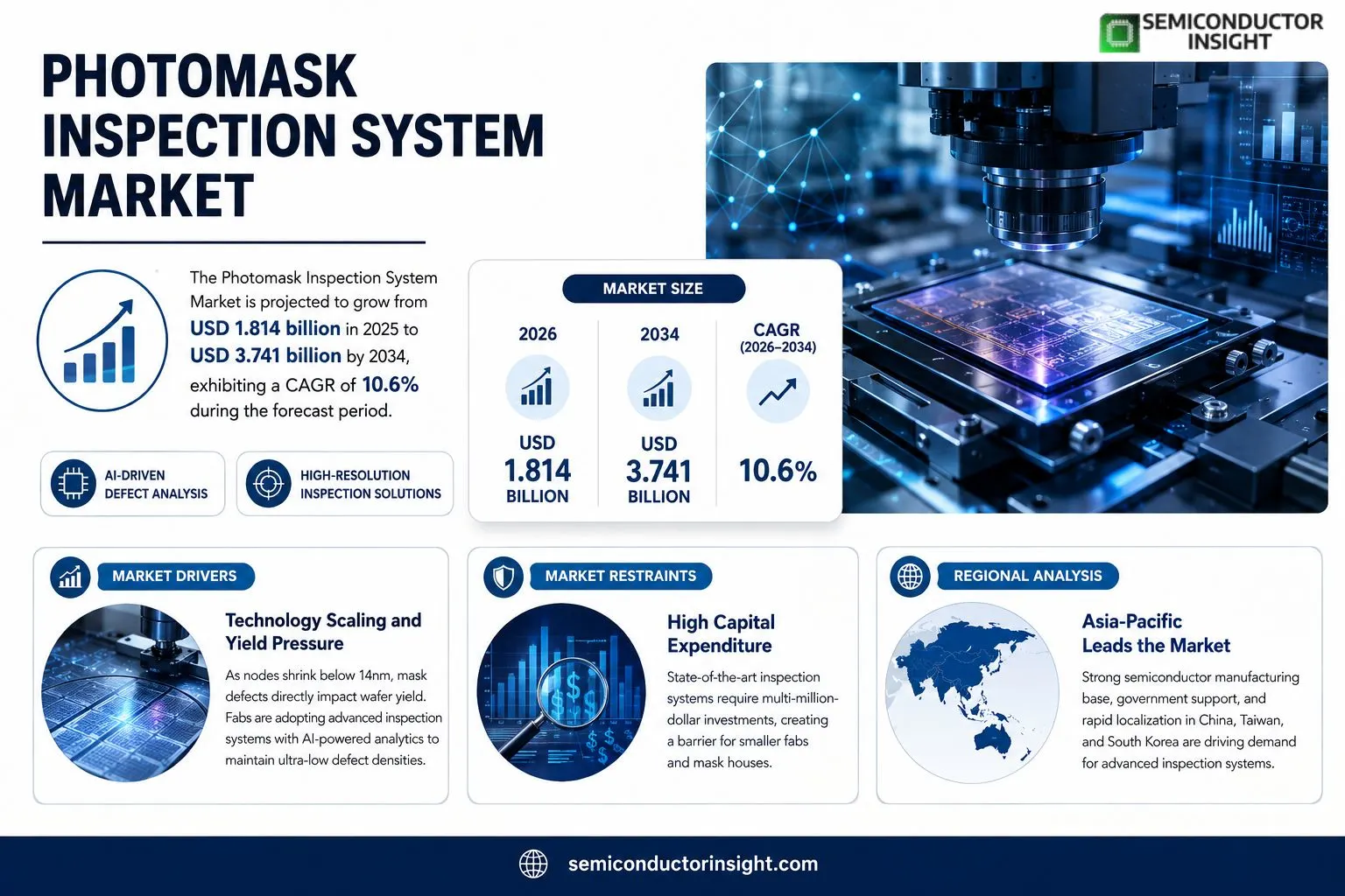
Photomask Inspection System market size was valued at USD 1.814 billion in 2025 and is forecasted to reach USD 3.741 billion by 2034, reflecting a CAGR of 10.6 % during the forecast period.
A photomask acts as the original master for transferring integrated‑circuit patterns onto semiconductor wafers; any lithography defect exceeding tolerance must be identified and corrected. Inspection systems employ high‑resolution imaging combined with sophisticated algorithms to spot sub‑micron anomalies, thereby safeguarding yield and performance throughout chip production.The market expands because AI compute chips demand ultra‑precise masks, high‑resolution displays push mask resolution limits, and emerging high‑NA EUV plus curved‑mask technologies introduce new inspection challenges. In Asia‑Pacificespecially Chinapolicy support accelerates domestic equipment sourcing, while AI‑based defect classification and full process automation improve accuracy and throughput.
MARKET DRIVERS
Technology Scaling and Yield Pressure
As semiconductor nodes shrink below 14 nm, pattern fidelity becomes a decisive cost factor. Photomask Inspection System Market participants are investing heavily in higher‑resolution sensors and AI‑augmented defect classification to keep defect densities within tolerable limits. The direct link between mask defects and downstream wafer yield forces fabs to adopt more rigorous inspection regimes, which in turn fuels equipment demand.
Regulatory and Quality Standards
International standards bodies have tightened acceptance criteria for mask defects, especially for advanced logic and memory devices. Companies that fail to meet these benchmarks risk costly re‑work or yield loss, prompting a swift upgrade of inspection capabilities. This regulatory climate creates a predictable stream of replacement and retrofit projects across the industry.
➤ Customers are prioritizing inspection platforms that integrate inline metrology, allowing real‑time feedback during mask production and reducing cycle time.
Overall, the confluence of sub‑10 nm scaling, stricter defect limits, and heightened compliance expectations translates into sustained orders for next‑generation inspection tools, shaping the revenue trajectory of Photomask Inspection System Market.
MARKET CHALLENGES
High Capital Expenditure
Acquisition costs for state‑of‑the‑art inspection systems often exceed several million dollars, creating a barrier for midsize fabs and mask houses operating on thin margins. The need to amortize these assets over relatively low production volumes can deter investment, especially in regions where funding is constrained.
Other Challenges
Skill Gap in Advanced Analytics
Deploying sophisticated defect detection algorithms requires personnel with deep knowledge of both optics and machine learning. The shortage of such talent slows down the effective rollout of newer inspection platforms, limiting the speed at which manufacturers can extract value from their capital outlays.
MARKET RESTRAINTS
Supply Chain Constraints
Component shortagesparticularly for high‑precision lenses and specialized sensorshave introduced lead times that exceed twelve months for many suppliers. This bottleneck curtails the ability of equipment manufacturers to meet order spikes, consequently limiting market expansion despite underlying demand.
Cost Sensitivity in Emerging Regions
Fabs in fast‑growing economies are increasingly price‑aware, opting for incremental upgrades rather than full‑scale replacements. This cautious spending pattern moderates overall market volume, especially where local financing mechanisms are underdeveloped.
MARKET OPPORTUNITIES
Hybrid Inspection Solutions
Combining optical and electron‑beam inspection within a single platform offers a compelling value proposition for manufacturers seeking comprehensive defect coverage without expanding floor space. Early adopters are reporting reduced downtime and improved defect traceability, suggesting a viable growth vector for equipment vendors.
Service‑Based Business Models
Offering inspection as a managed servicewhere providers retain ownership of high‑cost assets and charge per wafer or per defectcan lower entry barriers for smaller players. This model aligns revenue with usage, creating a recurring‑revenue stream that mitigates the impact of capital‑intensive purchases.
Photomask Inspection System Market Trends
Demand‑Driven: High‑Resolution Masks and AI Chip Boom
The surge in AI‑focused processors and ultra‑high‑definition display panels is reshaping the technical envelope of mask inspection equipment. Chip designers targeting sub‑7nm nodes require defect‑free masks that can transmit patterns with nanometer precision, compelling equipment suppliers to enhance sensor resolution and data‑processing bandwidth. Simultaneously, manufacturers of 4K/8K flat‑panel displays are pushing mask geometries toward finer pitches, which amplifies the need for inspection tools that can discern minute irregularities before lithography. This convergence of compute‑intensive chips and visual‑high‑end panels creates a market pressure that elevates purchasing urgency among semiconductor fabs and mask houses alike.
Other Trends
Technological Iteration: From EUV Masks to Curved Masks
Emerging lithography platforms such as high‑NA EUV impose novel optical challenges that existing inspection architectures struggle to resolve. Curved mask substrates, introduced to counter field‑flatness limitations, demand three‑dimensional metrology capabilities. Vendors are therefore integrating interferometric scanning and adaptive optics to capture surface topography across a curved plane, while also refining defect classification algorithms to account for altered diffraction patterns. This technical evolution not only widens the product portfolio but also raises the barrier to entry for newcomers lacking advanced optical expertise.
Regional Localization and Intelligent Upgrade
Geopolitical shifts and supply‑chain security concerns are accelerating the localization of inspection systems in the Asia‑Pacific, with China emerging as a focal point. Government incentives are encouraging domestic fabs to source inspection hardware locally, gradually reducing reliance on imported units. While current domestic mask‑blank production remains modest, policy‑backed investments are expanding the ecosystem of homegrown component suppliers, which in turn nurtures a fertile environment for regional system assemblers. Parallel to this, the industry is embedding artificial‑intelligence modules for defect discrimination and automating end‑to‑end workflows. AI‑enhanced image analysis shortens inspection cycles, improves yield forecasts, and frees operator time for higher‑value tasks. The combined effect of regional self‑sufficiency and intelligent automation positions Photomask Inspection System Market for a nuanced transformation that balances cost efficiency with technological sophistication.
COMPETITIVE LANDSCAPEKey Industry Players
Photomask Inspection System Market – Competitive Overview
The market is anchored by a handful of global integrators that combine metrology expertise with deep lithography know‑how. KLA Corp., headquartered in the United States, commands the largest share of high‑resolution EUV mask inspection equipment, leveraging its AI‑enhanced defect classification engine to meet the sub‑7 nm chip demand. Applied Materials complements KLA’s portfolio by offering a broader suite that spans both detection and substrate testing, allowing mask fabs to source end‑to‑end solutions from a single vendor. This duopoly creates a tiered structure where tier‑one firms dominate flagship projects for AI compute chips and premium display masks, while mid‑tier suppliers focus on volume‑driven nodes and legacy processes. The concentration limits price elasticity but also pushes smaller entrants to specialize in niche applications such as curved‑mask inspection or cost‑effective tooling for emerging regional fabs.
Beyond the two leaders, a diverse set of specialized players shapes the competitive field. Japan’s Lasertec and Advantest provide robust inspection platforms tailored for high‑NA EUV development, often collaborating with domestic semiconductor manufacturers. German‑based Carl Zeiss continues to profit from its optical expertise, delivering precision optics that underpin many inspection systems worldwide. Chinese firms including Visionoptech and NanoTech Instruments are rapidly scaling capacity under government‑backed localization programs, targeting domestic mask factories that seek alternatives to imported equipment. Smaller innovators such as NuFlare (Japan) and Tokyo Electron’s subsidiary MaskTech (Japan) focus on AI‑driven defect analytics, creating differentiation through software rather than hardware. The overall ecosystem reflects a balance between established global brands and agile regional specialists, each carving out value through technology focus, geographic positioning, or cost leadership.
List of Key Photomask Inspection System Companies Profiled
- KLA Corp.
- Applied Materials
- Lasertec Ltd.
- Carl Zeiss AG
- Advantest Corp.
- Visionoptech Co., Ltd.
- NuFlare Corp.
- NanoSys Technologies
- MaskTech (Tokyo Electron subsidiary)
- Nanotech Instruments (China)
- UltraMask Systems
- OptiInspect Ltd.
Segment Analysis:
| Segment Category | Sub-Segments | Key Insights |
| By Type |
|
By Type
|
| By Application |
|
By Application
|
| By End User |
|
By End User
|
| By Technology |
|
By Technology
|
| By Market Driver |
|
By Market Driver
|
Regional Analysis: Photomask Inspection System Market
Fab operators are favoring inspection systems that combine high‑NA optics with deep‑learning classifiers, enabling sub‑10nm defect detection without sacrificing throughput. Early adopters report noticeable yield improvements, prompting broader rollout across advanced process lines.
Vendors are embedding inspection data into Manufacturing Execution Systems, creating a closed loop that feeds real‑time quality metrics back to mask makers. This integration reduces rework cycles and aligns defect analytics with process controls.
Export‑control policies around high‑resolution imaging equipment have modestly tightened, encouraging domestic development of core components. The shift bolsters local supplier ecosystems and mitigates compliance risks for end users.
Established OEMs are defending market share through service contracts and software upgrades, while niche innovators target specialty nodes with bespoke inspection solutions, intensifying the battle for differentiated value.
Europe
European semiconductor fabs are leveraging Photomask Inspection System Market to meet EU‑driven sustainability mandates, emphasizing energy‑efficient equipment. Local manufacturers benefit from coordinated research programs that align optical hardware development with circular‑economy principles, helping them lower operational carbon footprints. Concurrently, the region’s fragmented market structure drives vendors to offer modular platforms that can be retrofitted, extending the lifespan of existing assets. This approach resonates with cost‑conscious players seeking to balance performance upgrades against capital constraints.
Asia‑Pacific
In Asia‑Pacific, the rapid expansion of fabs in China, Taiwan, and South Korea fuels demand for higher‑resolution inspection tools. Market participants are responding with aggressive localization strategies, establishing nearby engineering hubs to accelerate customizations. The competitive pressure compels suppliers to compress development cycles, delivering next‑generation optics within months rather than years. Additionally, regional governments are incentivising advanced mask‑inspection capabilities as part of broader semiconductor sovereignty agendas, creating a fertile environment for joint ventures.
South America
South America’s emerging semiconductor ecosystem remains modest, yet niche mask‑inspection services are gaining traction among research institutions and low‑volume specialty producers. The region’s limited capital availability encourages a focus on collaborative procurement models, where multiple stakeholders share access to high‑end inspection platforms. This cooperative stance mitigates upfront costs while still granting users exposure to state‑of‑the‑art defect detection, fostering incremental skill development across the market.
Middle East & Africa
Middle East & Africa exhibit nascent interest in photomask inspection, driven primarily by governmental push for diversification into high‑tech manufacturing. Early adopters are concentrating on pilot projects that integrate inspection systems with emerging fabs in the United Arab Emirates and South Africa. Partnerships with established vendors provide technology transfer pathways, allowing local teams to build competence in defect analytics. While the scale remains limited, the strategic emphasis on building a skilled workforce signals a long‑term intent to participate more fully in market.
Report Scope
This market research report provides a comprehensive analysis of Photomask Inspection System Market , covering the forecast period 2026–2034. It offers detailed insights into market dynamics, technological advancements, competitive landscape, and key trends shaping the industry.
Key focus areas of the report include:
- Market Overview: The report begins with an overview outlining its current market scenario, key growth indicators, and industry transformation drivers. It discusses macroeconomic factors, demand–supply balance, regulatory landscape, and the strategic role of semiconductors in powering advancements across industries such as automotive, telecommunications, consumer electronics, and industrial automation.
- Market Size & Forecast: Historical data and future projections for revenue, unit shipments, and market value across major regions and segments.
- Segmentation Analysis: Detailed breakdown by product type, technology, application, and end-user industry to identify high-growth segments and investment opportunities.
- Regional Insights: Insights into market performance across North America, Europe, Asia-Pacific, Latin America, and the Middle East & Africa, including country-level analysis where relevant.
- Competitive Landscape: Profiles of leading market participants, including their product offerings, R&D focus, manufacturing capacity, pricing strategies, and recent developments such as mergers, acquisitions, and partnerships.
- Technology Trends & Innovation: Assessment of emerging technologies, integration of AI/IoT, semiconductor design trends, fabrication techniques, and evolving industry standards.
- Market Drivers & Restraints: Evaluation of factors driving market growth along with challenges, supply chain constraints, regulatory issues, and market-entry barriers.
- Stakeholder Insights: Insights for component suppliers, OEMs, system integrators, investors, and policymakers regarding the evolving ecosystem and strategic opportunities.
Primary and secondary research methods are employed, including interviews with industry experts, data from verified sources, and real-time market intelligence to ensure the accuracy and reliability of the insights presented.
FREQUENTLY ASKED QUESTIONS:
What is the current market size of Photomask Inspection System Market?
-> Photomask Inspection System Market was valued at USD 1,814 million in 2025 and is expected to reach USD 3,741 million by 2034, at a CAGR of 10.6% over the forecast period.
Which key companies operate in Photomask Inspection System Market?
-> Key players include KLA (US), Applied Materials (US), Lasertec (JP), NuFlare (JP), Carl Zeiss AG (DE), Advantest (JP), Visionoptech (CN).
What are the key growth drivers?
-> Key growth drivers include the surge in demand for high‑resolution masks driven by AI compute chips and 4K/8K displays, technological iteration toward high‑NA EUV and curved masks, rapid localization and capacity expansion in the Asia‑Pacific region (especially China), and the integration of AI and automation to enhance inspection accuracy and throughput.
Which region dominates the market?
-> Asia‑Pacific holds the largest market share and is the fastest‑growing region, supported by strong semiconductor manufacturing activity and policy‑driven localization efforts, while Europe and North America remain important mature markets.
What are the emerging trends?
-> Emerging trends include AI‑enabled defect discrimination and data mining, full‑process automation, development of inspection solutions for high‑NA EUV lithography, and the adoption of curved mask inspection technologies to meet next‑generation lithography requirements.

Get Sample Report PDF for Exclusive Insights
Report Sample Includes
- Table of Contents
- List of Tables & Figures
- Charts, Research Methodology, and more...