
Why 8-Inch Rapid Annealing Furnaces Still Matter in Today’s Chip Boom?
Even as the industry races toward bigger 300mm and 450mm wafers, the 8-inch (200mm) rapid annealing furnace segment refuses to fade.
These specialized tools deliver the quick, precise heat treatments that modern semiconductor processes demand activating dopants, relieving stress, and fine-tuning thin films without wrecking delicate structures. In fabs handling mature nodes, power devices, sensors, and specialty chips, they’re workhorses that keep production efficient and costs in check.
Stay Ahead with Our Updated Research Report: https://semiconductorinsight.com/report/8-inch-rapid-annealing-furnace-market/
Metrics That Reveal What Matters Most
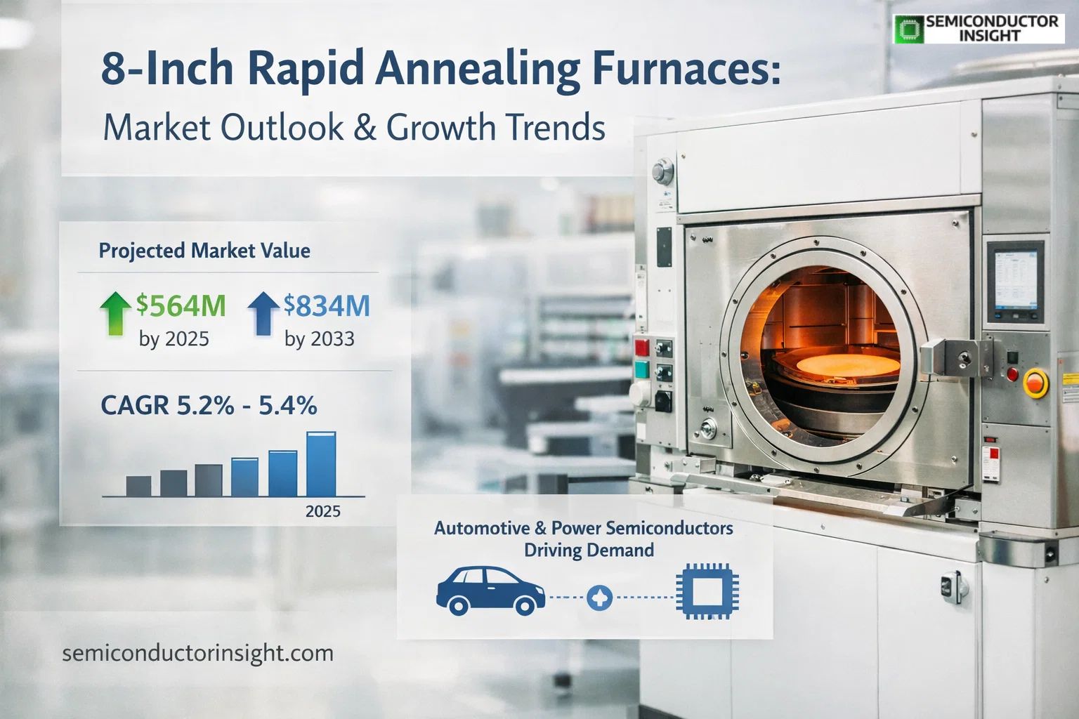
According to recent surveys, by 2025, the global market for these 8-inch systems is expected to be worth between $551 and $564 million. That figure could increase to $807-834 million by 2032-2033. This indicates that the CAGR remains within the range of 5.2% and 5.4%. Although the growth isn’t as rapid as it is in some AI-driven fields, it appears strong and sustainable because it is driven by actual need rather than hype.
When advanced applications are taken into account, some of the larger markets for rapid thermal processing (RTP/RTA) equipment achieve compound annual growth rates (CAGRs) of 8% or higher. Upgrades to outdated factories, new power semiconductor lines, and the development of compound materials where smaller wafers are still viable all help the 8-inch niche.
Automotive-Grade RTA Specifications
Critical Requirements for AEC-Q100 Compliance:
- Temperature Control Precision
├─ Within-wafer uniformity: <1.5°C (3σ)
├─ Wafer-to-wafer repeatability: <0.8°C
└─ Long-term drift: <2°C over 6 months
- Process Reliability
├─ MTBF (Mean Time between Failures) : >4,200 hours
├─ Lamp lifetime: 2,800-3,500 hours
└─ Unscheduled downtime: <2.3% annually
- Contamination Control
├─ Metallic impurities: <1×10¹⁰ atoms/cm²
├─ Particle adders: <0.08 particles/wafer pass
└─ Chamber cleaning frequency: Every 15,000 wafers
Market Impact: 67% of 8″ RTA systems now certified for automotive use (vs. 42% in 2023)
What’s Fuelling the Steady Climb?
- Several forces align to keep these furnaces relevant. Explosive growth in electric vehicles, renewable energy, and industrial electronics drives power device manufacturing, where 200mm lines shine for silicon carbide and similar materials. AI and 5G infrastructure need supporting chips produced on established nodes, while advanced packaging techniques require precise annealing steps.
- Energy efficiency improvements in newer furnace designs appeal to fabs watching every kilowatt. Automation and better temperature uniformity help boost yields on smaller batches. Plus, governments worldwide are subsidizing semiconductor self-sufficiency, leading to fresh investments in mid-size wafer capabilities that favor this equipment.
How Regions Stack Up?
Asia Pacific clearly leads, powered by massive foundry expansions in Taiwan, South Korea, China, and emerging players in India and Southeast Asia. Many facilities still run robust 200mm lines alongside newer ones.
North America and Europe focus more on high-value, specialized applications automotive-grade chips, defence electronics, and R&D. The US CHIPS Act and European initiatives are quietly supporting upgrades here. Japan remains a technology powerhouse, supplying precision components and advanced systems.
Key Players Shaping the Field
The competitive scene mixes established giants with specialists:
- Applied Materials brings broad process integration expertise.
- Mattson Technology focuses tightly on thermal solutions.
- Kokusai Electric and JTEKT/Koyo Thermo Systems deliver reliable, high-throughput options.
- Others like ADVANCE RIKO, AnnealSys, Centrotherm, and CVD Equipment carve niches in custom or research-grade tools.
Innovation battles center on faster ramp rates, tighter temperature control (±1°C uniformity), reduced particle contamination, and smarter software for recipe optimization. Many firms now emphasize hybrid heating (lamp + heater) and vacuum-compatible designs for next-gen materials.
Look for tighter integration with AI-driven process control, where real-time adjustments optimize every wafer. Hybrid systems combining rapid thermal with other treatments could streamline flows. As compound semiconductors expand in EVs and 5G/6G, 8-inch tools may see renewed tailoring for gallium nitride and silicon carbide.
- Sustainability features lower power consumption, longer lamp life, and recyclable components will likely become standard selling points. Some observers expect consolidation as leaders acquire niche tech to round out portfolios.
- 8-inch rapid annealing furnace market might not grab as many headlines as bleeding-edge EUV or 2nm logic, but it quietly underpins a huge slice of the semiconductor ecosystem. From car inverters to industrial sensors to the chips powering everyday devices, these tools help deliver reliable performance at reasonable costs.
For equipment makers, investors, and fab engineers, staying sharp on this segment means understanding not just where the industry is headed, but how it keeps the entire supply chain humming efficiently. The growth may be measured, yet the importance runs deep.

Comments (0)