

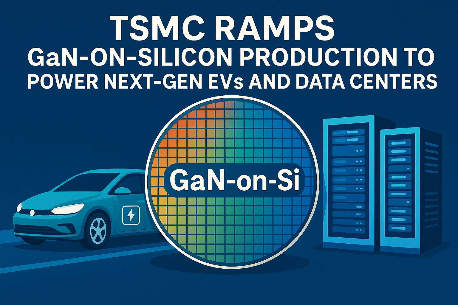
TSMC Ramps GaN-on-Silicon Production to Power Next-Gen EVs and Data Centers
For decades, silicon reigned as the cornerstone of modern electronics. From computers and smartphones to solar panels and electric vehicles, nearly every device we touch relies on silicon-based chips. But as the world demands faster, smaller, and more energy-efficient devices, silicon is starting to show its limits.
Enter Gallium Nitride (GaN), a wide-bandgap semiconductor that promises to redefine power electronics and radio-frequency (RF) applications. GaN’s unique properties high breakdown voltage, superior thermal conductivity, and fast switching speeds make it an ideal candidate for next-generation chargers, electric vehicles, 5G base stations, satellites, and even AI data centers.
The numbers speak volumes: the Gallium Nitride semiconductor devices, substrates, and wafers market was valued at USD 2,371 million in 2024 and is projected to soar to USD 7,690 million by 2032, growing at a remarkable CAGR of 18.8%. This rapid expansion underscores both technological breakthroughs and surging demand across industries.
Access Your Free Sample Report- Gallium Nitride Semiconductor Devices, Substrate and Wafer Market
Industry and Manufacturing Breakthroughs
TSMC Expands Its GaN Roadmap
Taiwan Semiconductor Manufacturing Co. (TSMC), the world’s largest contract chipmaker, recently accelerated its GaN-on-Silicon production. DigiTimes reported in June 2024 that TSMC is now producing 650V GaN-on-Si power devices for applications such as EV chargers, renewable energy inverters, and hyperscale data centers.
Why is this significant? Historically, GaN was limited to niche RF devices and smaller-scale production. TSMC’s move indicates that GaN is graduating into mainstream semiconductor manufacturing. By offering GaN processes alongside its silicon technologies, TSMC enables fabless companies to design GaN devices without building their own specialized fabs. This democratizes access and accelerates adoption.
Intel’s Push Into GaN for AI Servers
Intel, best known for its CPUs, has begun exploring GaN for AI data center power delivery systems. EE Times reported in July 2024 that Intel is collaborating with GaN suppliers to integrate the technology into server power modules.
Here’s the catch: AI training workloads demand massive computational power, which translates to high energy consumption. Traditional silicon-based MOSFETs generate significant heat and inefficiencies. GaN devices, with their fast switching and low power loss, could cut data center energy usage dramatically an essential step as hyperscale operators face mounting pressure to reduce their carbon footprint.
STMicroelectronics and GlobalFoundries’ GaN Venture
In May 2024, Reuters confirmed that STMicroelectronics and GlobalFoundries are joining forces to build a GaN-focused fab in Catania, Italy. Backed by EU Chips Act funding, the facility will produce GaN power devices for automotive and industrial applications.
This partnership is strategic for two reasons:
- It anchors GaN manufacturing within Europe, reducing reliance on Asian foundries.
- It addresses the growing need for GaN in electric mobility (EV onboard chargers, inverters) and industrial efficiency (robotics, smart grids).
Applications Driving GaN Adoption
Apple’s GaN Chargers: Compact Powerhouses
Bloomberg reported in February 2024 that Apple is scaling up GaN-based USB-C chargers for its next generation of MacBooks. Apple’s move is no surprise GaN allows for chargers that are smaller, lighter, and more efficient than their silicon counterparts.
The significance extends beyond Apple. Once a global consumer electronics leader adopts GaN en masse, it sets a precedent for the rest of the industry. This could accelerate GaN’s entry into laptops, tablets, and even gaming consoles.
Tesla’s EV Chargers Eye GaN Integration
Electrek revealed in March 2024 that Tesla is exploring GaN technology for on-board EV chargers. Current silicon-based chargers face heat management and efficiency bottlenecks. By integrating GaN, Tesla could:
- Reduce charger size and weight, improving vehicle range.
- Shorten charging times, a key consumer concern.
- Boost energy efficiency, aligning with Tesla’s sustainability mission.
If Tesla succeeds, other EV makers will likely follow, further embedding GaN into the automotive supply chain.
AI GPUs and Data Center Power Shifts
In April 2024, AnandTech reported that both Nvidia and AMD suppliers are transitioning to GaN-based power management modules for GPUs. AI training consumes megawatts of power per cluster, and GaN’s fast-switching devices help reduce conversion losses.
This is not just a performance story it’s an environmental one. As AI demand skyrockets, governments and corporations alike are under scrutiny for energy-intensive computing. GaN could be the efficiency enabler that keeps AI growth sustainable.
Download Sample Report PDF- Gallium Nitride Semiconductor Devices, Substrate and Wafer Market
Substrate and Wafer Innovations
Japan’s NIMS Achieves Breakthrough in GaN Substrates
The National Institute for Materials Science (NIMS) in Japan reported in August 2024 that it had achieved ultra-low defect density GaN wafers using an improved hydride vapor phase epitaxy (HVPE) method.
This breakthrough is critical because GaN substrates have historically suffered from high defect rates, limiting yield and raising costs. NIMS’ process could enable larger-diameter wafers (up to 8 inches), paving the way for high-volume production at reduced costs.
Soitec Launches 200mm GaN-on-Si Wafers
In September 2024, EE News Europe reported that Soitec began volume production of 200mm GaN-on-Si engineered substrates. Larger wafer sizes translate directly into economies of scale. Foundries using Soitec’s wafers can now produce more chips per batch, driving down unit costs.
This development also makes GaN more competitive with silicon carbide (SiC), another wide-bandgap material. While SiC is favored in high-voltage EV inverters, GaN is carving out territory in consumer chargers, renewable energy, and AI power systems.
Policy, Defense, and Investment Trends
U.S. Defense Department Expands GaN Use
In January 2024, Defense News reported that the U.S. Department of Defense (DoD) expanded contracts for GaN-based RF devices in radar, satellite communications, and missile defense.
GaN’s high-frequency performance and radiation hardness make it superior for military and aerospace systems. As geopolitical tensions rise, GaN’s role in securing communications and enhancing radar resolution will only grow.
Europe Bets on GaN Through the EU Chips Act
The EU Chips Act has earmarked billions in subsidies for semiconductor capacity, with GaN being a key beneficiary. In May 2024, the Financial Times confirmed that Infineon, STMicroelectronics, and Aixtron are receiving support to scale GaN fabs across Europe.
This aligns with Europe’s broader goal of achieving semiconductor sovereignty while simultaneously advancing clean energy and EV infrastructure.
Market Outlook and Strategic Implications
Growth Trajectory
The GaN semiconductor market’s projected growth from USD 2.37 billion in 2024 to USD 7.69 billion by 2032 (CAGR: 18.8%) reflects three converging forces:
- Technological Maturity: Substrate innovations and 200mm wafer launches are lowering costs.
- Application Expansion: From consumer chargers to EVs and AI servers, GaN is moving mainstream.
- Policy Support: Government investments in defense and industrial capacity are accelerating adoption.
GaN vs. Silicon Carbide (SiC)
While both GaN and SiC are wide-bandgap semiconductors, they are not direct substitutes. Instead, they complement each other:
- GaN: Best suited for high-frequency, lower-voltage (<1,000V) applications like chargers, data centers, and RF systems.
- SiC: Excels in high-voltage (>1,000V) power electronics, particularly EV traction inverters and utility-scale renewable grids.
Investors and manufacturers should view GaN as part of a dual-material future, not a single-material replacement for silicon.
Click Here To Download Full Sample Report- Gallium Nitride Semiconductor Devices, Substrate and Wafer Market
Investment Hotspots
- Consumer Electronics: Compact fast chargers remain the entry point for mass GaN adoption.
- Electric Vehicles: On-board chargers and DC fast-charging stations are the next growth engines.
- Data Centers & AI: Power-hungry GPUs will rely on GaN for sustainable expansion.
- Defense & Aerospace: RF and satellite systems will continue to push GaN’s high-frequency limits.
As we look toward 2032, GaN’s combination of efficiency, performance, and scalability could make it as foundational as silicon was in the 20th century. And with a projected market value approaching $8 billion, the semiconductor industry and the world at large is betting big on GaN’s promise.

Comments (0)