

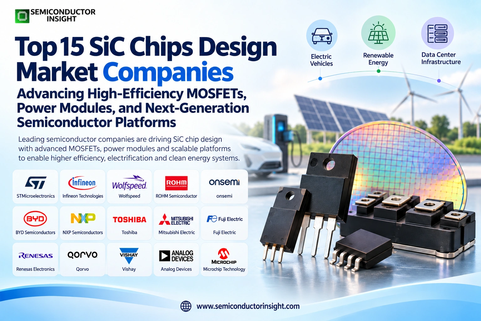
Top 15 SiC Chips Design Market Companies Advancing High-Efficiency MOSFETs, Power Modules, and Next-Generation Semiconductor Platforms
Silicon carbide (SiC) chip design is becoming a critical discipline in power electronics as electric vehicles, fast-charging infrastructure, renewable-energy converters and industrial drives demand higher efficiency at elevated voltages and temperatures.
SiC MOSFETs and Schottky diodes can enable high-voltage switching with lower switching losses than conventional silicon devices when used in appropriately designed circuits. However, achieving these benefits requires more than the material alone. Real-world performance depends on design, including device architecture, gate-oxide reliability, packaging parasitics, thermal management and gate-drive compatibility.
STMicroelectronics: Expanding SiC Design Flexibility across EV Voltage Platforms
STMicroelectronics stands out for the breadth of its SiC MOSFET portfolio, which spans 650 V to 2,200 V and addresses automotive and industrial power conversion. Its published catalogue includes devices for traction inverters, onboard chargers and DC-DC converters, with packaging options such as HiP247, H2PAK-7, STPAK and HU3PAK.
- This variety matters because designers must balance electrical performance with PCB footprint, cooling requirements and insulation distances.
- For example, ST lists a 1,200 V automotive-grade device rated at 40 A with a typical on-resistance of 40 milliohms, while higher-current STPAK devices serve more demanding power stages.
- Its competitive advantage lies in giving engineers multiple voltage, current and packaging combinations within one design ecosystem.
Infineon Technologies: Moving SiC Device Design toward Larger Wafer Platforms
Infineon is strategically important because its SiC programme combines device design, power modules and manufacturing scale. On October 15, 2026, it announced a multiyear agreement with Wolfspeed to source 200 mm SiC wafers, supporting its transition from 150 mm substrates to the larger format. Larger wafers can accommodate more device dies per wafer, although the economic benefit depends on die size, defect density, processing yield and manufacturing costs.
The agreement also strengthens substrate supply flexibility for electric vehicles, renewable-energy systems and AI data-centre power infrastructure. For design teams, the transition creates a pathway to higher-volume production, but maintaining stable device performance and qualification standards during manufacturing migration remains critical.
Wolfspeed: Pushing SiC Design into Medium- and High-Voltage Power Systems
Wolfspeed is particularly relevant to SiC chip design because its activities span substrates, epitaxial materials and power devices. On March 5, 2026, it announced a commercially available 10,000 V SiC power MOSFET, targeting grid modernisation, industrial electrification and high-power infrastructure. It subsequently introduced two 3.3 kV SiC power-module families in May and Gen 5 SiC MOSFET technology in June.
- The Gen 5 announcement highlighted improvements in specific on-resistance and reported up to 27% efficiency improvement over competing 1,200 V solutions under the company’s stated comparison conditions.
- These developments illustrate a shift beyond the conventional EV inverter market toward medium-voltage power conversion and demanding industrial applications.
ROHM Semiconductor: Improving Switching Performance through Trench MOSFET Architecture
ROHM’s fourth-generation SiC MOSFETs demonstrate how chip architecture can improve performance without simply increasing the die size. Its official product specifications report approximately 40% lower on-resistance and 50% lower switching loss compared with conventional products in the company’s stated comparison. The 1,200 V SCT4018KW7, for example, is rated at 75 A, with a typical on-resistance of 18 milliohms and a maximum junction temperature of 175°C.
ROHM also offers automotive-qualified trench devices, including variants meeting AEC-Q101 requirements. These specifications are useful to engineers comparing inverter efficiency, conduction losses, thermal limits and gate-drive requirements. The important differentiator is the combination of device structure, electrical ratings and qualification options rather than voltage rating alone.
onsemi: Linking SiC Device Selection with Simulation and System Design
onsemi is strengthening its SiC proposition by helping engineers evaluate complete power-stage combinations rather than choosing transistors in isolation. On June 8, 2026, the company introduced its Elite Pairing Studio, an interactive design environment for evaluating SiC MOSFET and gate-driver pairings. The tool exposes switching behaviour, timing and performance trade-offs early in the design process, helping engineers identify potential issues before full system testing.
This is particularly relevant to EV traction systems, industrial power supplies and AI data-centre infrastructure, where switching losses, electromagnetic interference and thermal behaviour interact. On October 14, 2026, onsemi also announced that Sungrow had adopted its SiC hybrid power-module technology for the PowerTitan 3.0 energy-storage platform. Together, these developments show the importance of combining semiconductor design with application-level optimisation.
To Know More about the Report, You Can Freely Browse Our Latest Updated Report: https://semiconductorinsight.com/report/sic-chips-design-market/
BYD Semiconductor: Aligning SiC Devices with Electric-Vehicle Powertrain Integration
BYD Semiconductor is relevant to SiC chip design because it operates close to the vehicle architectures in which power semiconductors are deployed. For electric vehicles, SiC devices can be used in traction inverters, onboard charging systems and high-voltage power conversion, where switching efficiency and thermal management influence system performance.
BYD’s broader vehicle and electronics integration provides a potential advantage in matching semiconductor characteristics to actual powertrain requirements. However, the company’s overall semiconductor activity should not be treated as equivalent to independently verified SiC chip-design market share. For a rigorous supplier assessment, the most useful evidence would include SiC die specifications, production volumes, vehicle-platform adoption and the proportion of powertrain applications using SiC rather than silicon-based devices.
Microchip Technology: Bringing 3.3 kV SiC Devices into AI Data-Centre Power Architectures
Microchip has opened a new application area for SiC power design through its medium-voltage power modules. On May 26, 2026, it announced 3.3 kV HV-D3 mSiC power modules intended for solid-state transformers used in AI hyperscale data centres and other high-voltage systems. The modules integrate SiC MOSFETs and Schottky diodes in a standard 62 mm package.
That package format can simplify mechanical integration and thermal design for power-electronics developers. Solid-state transformers use high-frequency power conversion to manage electricity between voltage levels, offering potential advantages in system flexibility and power density. Microchip’s product direction demonstrates how SiC design is expanding beyond vehicle inverters into grid-connected equipment, industrial conversion and data-centre power distribution.
Mitsubishi Electric: Extending SiC Module Design across Traction and Industrial Voltage Classes
Mitsubishi Electric combines SiC device technology with power-module engineering for applications ranging from electric vehicles to railway systems and industrial drives. Its published portfolio includes full-SiC modules rated from 1,200 V to 1,700 V, with current ratings spanning 300 A to 1,200 A, alongside high-voltage modules rated up to 3,300 V.
In October 2025, the company completed a new factory building for 200 mm SiC wafer production in Kumamoto, Japan, and reported that it was accelerating the production-line ramp-up. The company also announced sample shipments of full-SiC and hybrid-SiC SLIMDIP modules in April 2025 for energy-saving appliances. These developments connect chip design with manufacturing scale and module-level integration, two important requirements for broadening SiC adoption.
SEMIKRON Danfoss: Turning SiC Chip Performance into Practical Power Modules
SEMIKRON Danfoss plays a key role in the SiC design ecosystem by integrating semiconductor dies into power modules engineered for demanding electrical and thermal environments. Its packaging approach is particularly important in renewable-energy converters, industrial motor drives and high-power inverters, where parasitic inductance and thermal resistance can undermine the benefits of fast-switching devices.
In June 2026, the company announced a new standard power-module package developed with Mitsubishi Electric, combining the SEMITRANS 20 and LV100 package concepts. The design supports three-level circuit configurations and is intended for IGBT and SiC technologies up to 3.3 kV. This emphasis on standardised interfaces can help equipment manufacturers simplify inverter designs and diversify their component supply chains.
Fuji Electric: Reducing Module Size through Three-Dimensional Interconnection
Fuji Electric’s SiC strategy highlights the importance of packaging architecture alongside semiconductor performance. In its FY2025 annual-report materials, the company described a new SiC module using three-dimensional wiring technology that is 49% smaller than conventional products. The approach reduces internal inductance, which can help control voltage overshoot and switching behaviour in high-speed power circuits.
Fuji Electric planned to begin mass production of the compact SiC module in fiscal 2026. This matters in electric-vehicle powertrains, where inverter packaging must accommodate limited space, demanding thermal conditions and stringent reliability requirements. The stated size reduction is a company-reported comparison, so engineers should assess the final module against equivalent current ratings, cooling conditions and electrical performance before drawing system-level conclusions.
Navitas Semiconductor and GeneSiC: Targeting High-Voltage Switching and Fast Power Conversion
Navitas brings the GeneSiC technology portfolio into a power-semiconductor strategy that addresses high-voltage conversion, industrial systems and fast-charging applications. SiC MOSFETs are particularly relevant in circuits where high blocking voltage and lower switching losses can reduce conversion-stage losses and cooling requirements. GeneSiC’s product engineering is therefore relevant to power supplies, renewable-energy converters and industrial drives, where designers must balance on-resistance, gate charge, switching energy and short-circuit robustness.
The commercial distinction is that device performance depends on the complete circuit and operating conditions, not only the headline voltage rating. In July 2026, Wolfspeed filed a patent-infringement lawsuit against Navitas, adding an important intellectual-property development to the competitive landscape. The filing itself should not be interpreted as a legal finding against Navitas.
Qorvo and UnitedSiC: Using SiC FET Architectures to Simplify Power Conversion
UnitedSiC’s technology, now associated with Qorvo’s acquired power-semiconductor portfolio, is known for SiC FET designs that combine a SiC JFET with a silicon MOSFET in a cascode configuration. This architecture can offer a normally-off device with gate-drive characteristics familiar to many power-electronics designers. The approach is relevant to high-efficiency AC-DC converters, EV charging equipment, server power supplies and industrial power conversion.
Its value is not simply the use of SiC, but the way device architecture affects switching behaviour, gate-drive compatibility and circuit protection. For buyers, comparisons should include reverse-conduction behaviour, switching losses at the intended frequency and voltage, and short-circuit performance. Current product availability and ownership of specific product families should be verified against Qorvo’s latest catalogue before publication.
San’an Optoelectronics: Building a Broader SiC Manufacturing Ecosystem in China
San’an Optoelectronics is relevant to the Chinese compound-semiconductor ecosystem through its investment in wide-bandgap semiconductor capabilities. SiC manufacturing requires coordinated development of substrates, epitaxial layers, wafer processing and device qualification, and these capabilities influence how quickly a supplier can progress from prototype devices to repeatable commercial production. San’an’s importance should be evaluated through its power-device product releases, manufacturing qualifications and customer adoption rather than through its broader LED or optoelectronics business.
In 2026, the key questions for buyers are whether specific SiC MOSFET or diode products are available in production quantities, which voltage classes they cover, and whether they have completed qualification for automotive or industrial applications. Publicly comparable SiC device-volume figures are not consistently disclosed, so precise production rankings would require further confirmation.
Littelfuse and IXYS: Connecting SiC Devices with Protection and Power-System Design
Littelfuse’s relevance to SiC power electronics comes from the combination of its power-semiconductor portfolio and expertise in circuit protection. The IXYS product heritage includes power switches, diodes and module technologies that can complement modern SiC-based power stages. In practical designs, SiC MOSFETs can switch rapidly enough that circuit layout, overvoltage protection and gate-drive design become especially important. This creates a role for suppliers that can support both the switching device and the surrounding protection architecture.
For engineering teams, the useful comparison is not simply the number of SiC products available, but the range of voltage ratings, package formats, thermal limits and protection components that can be integrated into a reliable system. The current status of individual IXYS-branded SiC products should be checked against Littelfuse’s latest technical documentation.
CETC 55: Strengthening China’s Domestic SiC Device Design Capabilities
CETC 55, associated with China’s compound-semiconductor research and manufacturing ecosystem, is relevant to SiC development because domestic capability depends on more than wafer availability. Device design, epitaxial quality, defect control, process integration and reliability testing all determine whether a SiC component can meet demanding power-electronics specifications.
These capabilities are important for industrial drives, power supplies and other high-voltage applications where device consistency affects system qualification. Its position should be evaluated through verifiable SiC device datasheets, demonstrated voltage and current ratings, manufacturing qualifications and disclosed application deployments.

Comments (0)