
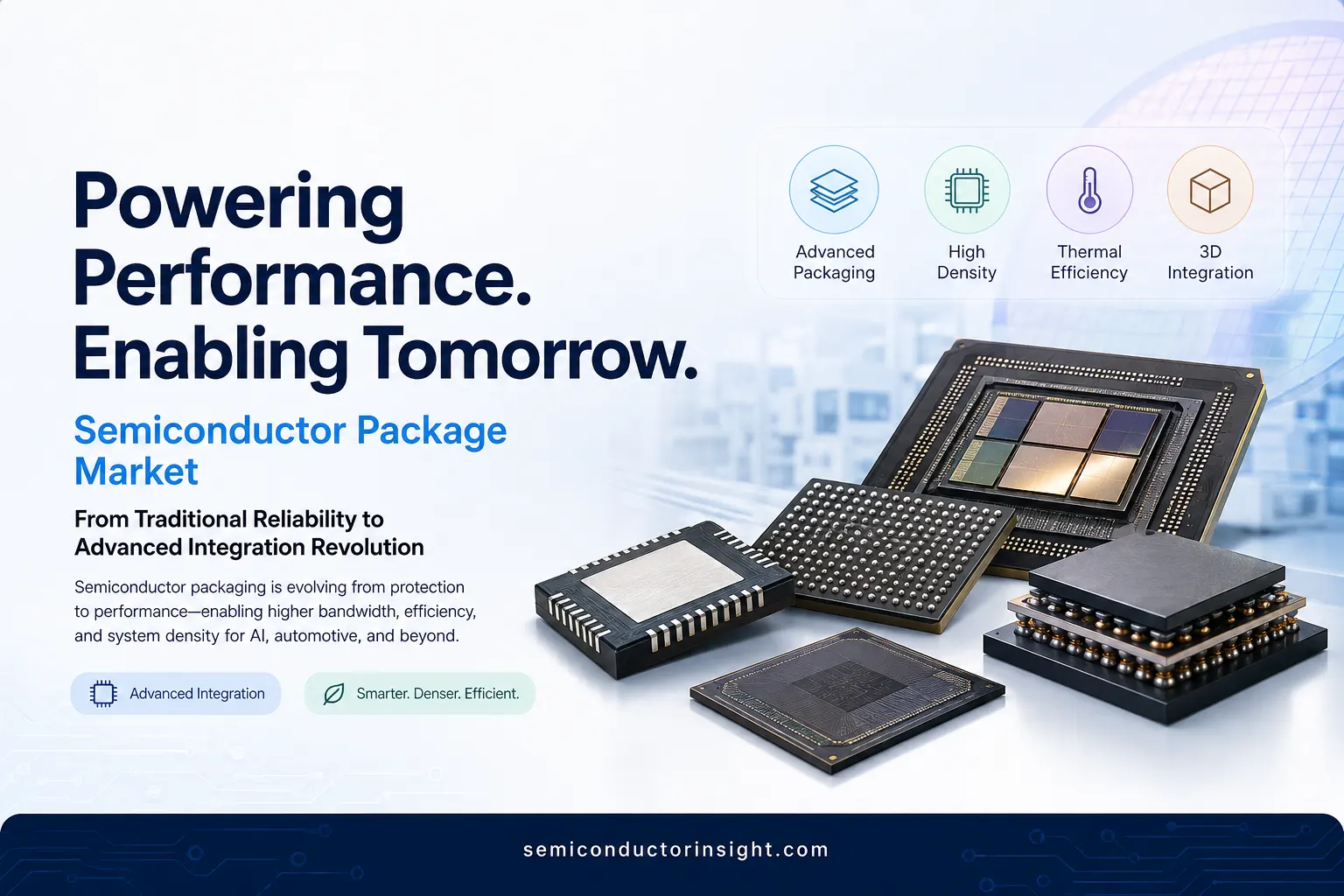
Top Leading Classifications Defining semiconductor package market Landscape across AI HPC and Next-Generation Devices
Semiconductor packaging has evolved from simple protective enclosures into a critical performance enabler that determines bandwidth, power efficiency, and system density. Global silicon wafer shipments reached 12,973 million square inches in 2025, reflecting sustained demand that packaging must match through both traditional and advanced formats. The industry now balances high-volume legacy packages with sophisticated multi-die solutions required for AI accelerators and high-performance computing.
- Traditional leadframe packages continue serving cost-sensitive applications where moderate pin counts suffice. These structures support reliable interconnects for many consumer and industrial chips while offering mature assembly processes that handle tens of millions of units monthly across global facilities.
- Quad Flat No-lead designs deliver compact footprints and improved thermal paths for mobile and automotive controllers, eliminating external leads to reduce package size and improve board-level reliability under vibration. Ball Grid Array formats remain foundational for mid-range processors, providing dense solder-ball arrays that accommodate hundreds of connections while managing heat through substrate pathways.
- Fan-out packaging expands available interconnect area beyond the die footprint itself. This approach places redistribution layers around the chip, enabling higher I/O counts without enlarging the silicon. Demand has intensified for server and networking chips that require dense signal routing within constrained board space. Two-point-five-dimensional packaging uses silicon interposers to link multiple dies side-by-side with fine-pitch microbumps, creating short, high-bandwidth pathways essential for pairing logic with high-bandwidth memory
- Three-dimensional stacking builds vertically through hybrid bonding or through-silicon vias, dramatically increasing transistor density and reducing signal latency between layers. System-in-Package solutions integrate processors, memory, and passive components into a single module, simplifying board design for space-constrained consumer devices and automotive modules.
- AI and high-performance computing data centers represent the most intensive application domain. Accelerators and GPUs increasingly rely on advanced packages to deliver the interconnect density needed for massive parallel workloads. Packaging capacity for chip-on-wafer-on-substrate technologies has expanded rapidly, with industry projections pointing toward demand approaching one million wafers by 2026 to support successive generations of AI platforms.
- Automotive electronics demand packages capable of surviving extreme temperature cycles and delivering consistent power efficiency for electric vehicle powertrains and advanced driver-assistance systems. Consumer mobile devices continue to push miniaturization, favoring lead-less and fan-out formats that fit thinner form factors while maintaining thermal performance under sustained loads.
Interconnect Density and Hybrid Bonding Pathways
The progression from microbump to bumpless hybrid bonding marks a decisive shift. Hybrid bonding achieves finer pitches that support the bandwidth requirements of next-generation processors. TSMC has advanced CoWoS interposer sizes from earlier reticle limits toward larger 5.5-reticle configurations while qualifying face-to-face and face-to-back SoIC stacking processes for production. These techniques allow multiple logic and memory layers to communicate with minimal parasitics. Intel’s EMIB and Foveros approaches similarly enable heterogeneous integration, with large-scale packaging facilities supporting external customers alongside internal needs.
Capacity Flow and Expansion Map
A simplified flow illustrates the packaging pathway: Wafer fabrication → Die preparation → Interposer or redistribution layer formation → Hybrid bonding or microbump attach → Substrate assembly → Thermal interface application → Final test and system integration.
Capacity expansions focus on both front-end stacking and back-end substrate processes. Monthly CoWoS output has scaled from earlier tens of thousands of wafers toward significantly higher volumes, yet demand from leading AI designers continues to book substantial portions of available slots. Memory makers simultaneously expand high-bandwidth memory stacking capacity to match logic packaging throughput.
Thermal and Reliability Considerations across Segments
Advanced packages address power density challenges through improved heat-spreading materials and optimized thermal interfaces. Automotive qualification requires packages to endure thousands of temperature cycles while maintaining electrical integrity.
Data-center modules prioritize both peak performance and sustained efficiency under continuous high loads. These requirements drive collaboration between foundries, OSATs, and system designers to qualify new material stacks and bonding processes ahead of volume ramps.
To find out more, feel free to browse our latest updated report: https://semiconductorinsight.com/report/semiconductor-package-market/
Recent Deployment Instances
Major AI platforms from leading designers have secured large allocations of advanced packaging capacity for successive accelerator generations. Apple’s recent processor packages incorporate face-to-face hybrid bonding for consumer computing performance.
Automotive suppliers integrate system-in-package modules for sensor fusion and power management units. Public research efforts, including growth-based monolithic three-dimensional techniques demonstrated at institutions such as MIT, explore pathways to stack dozens of layers with improved alignment and density.
Package Type Comparison Snapshot
Semiconductor packages range from cost-effective leadframe/QFN designs for mobile and industrial uses to advanced 3D hybrid-bonded stacks for high-performance computing. Mid-tier options like BGA and fan-out support processors and networking gear with balanced density or expanded I/O, while 2.5D interposer-based packages deliver the high bandwidth essential for AI accelerators.
Semiconductor package market continues to advance through material innovation, process refinement, and capacity scaling that directly enable higher system performance. From traditional formats supporting everyday electronics to sophisticated multi-die assemblies powering AI infrastructure, packaging remains the essential bridge between silicon capability and real-world application demands.

Comments (0)