
Top Chiplets Market Trends: The Shift toward Disaggregated Silicon Design
A Structural Shift in Semiconductor Design
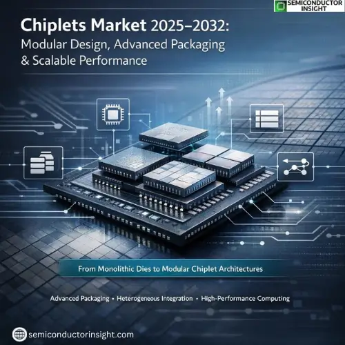
The semiconductor industry is undergoing a fundamental architectural transition, driven by escalating design complexity, rising fabrication costs, and the physical limits of transistor scaling. Within this context, chiplets have emerged as a structural solution rather than an incremental innovation. Instead of building ever-larger monolithic dies, manufacturers are increasingly adopting modular chiplet-based designs that combine multiple smaller dies into a single package.
Chiplets allow semiconductor designers to break down complex
https://semiconductorinsight.com/report/audio-system-on-chip-market/
architectures into function-specific silicon blocks, each optimized for performance, yield, and process node selection. This approach is reshaping how processors, accelerators, and high-performance computing platforms are conceived and manufactured.
Defining Chiplets in Semiconductor Architecture
- In semiconductor terms, a chiplet is a disaggregated functional die designed to work as part of a larger integrated package.
- Each chiplet may serve a dedicated purpose compute, memory, I/O, interconnect, or specialized acceleration and is connected through advanced packaging technologies such as 2.5D interposers or 3D stacking.
- This architectural model enables designers to mix and match silicon built on different process nodes.
- For example, leading-edge logic may coexist with mature-node analog or I/O chiplets, creating cost-efficient yet high-performance systems. The result is greater design flexibility without compromising system integration.
Why Chiplets Matter to the Semiconductor Ecosystem?
The adoption of chiplets directly addresses several long-standing challenges in semiconductor manufacturing. Yield loss becomes increasingly problematic as die sizes grow larger; chiplets mitigate this by keeping individual die sizes smaller and easier to manufacture. This leads to higher overall yield and improved cost control, especially for advanced nodes.
Chiplets also shorten development cycles. Design teams can reuse validated chiplet IP across multiple product generations, reducing time-to-market and engineering risk. This reusability is particularly valuable in data-centre processors, AI accelerators, and custom silicon platforms where rapid iteration is critical.
Advanced Packaging as the Market Enabler
Chiplets Market is inseparable from progress in advanced semiconductor packaging. Technologies such as silicon interposers, fan-out wafer-level packaging (FOWLP), and through-silicon vias (TSVs) are foundational to enabling low-latency, high-bandwidth communication between chiplets.
Packaging houses and foundries are investing heavily in heterogeneous integration capabilities, recognizing that packaging performance now rivals transistor performance as a differentiator. This shift has elevated packaging from a backend operation to a strategic element of semiconductor design.
Major Inventions & Developments
January 2026: Cadence announced a Chiplet Spec-to-Packaged Parts ecosystem to reduce engineering complexity and accelerate time to market for customers developing chiplets targeting physical AI, data center, and high-performance computing (HPC) applications. Arm, Arteris, eMemory, M31 Technology, Silicon Creations, Trilinear Technologies, and silicon analytics partner proteanTecs are among the first IP partners to join Cadence. Cadence and Samsung Foundry are working together to develop a silicon prototype demonstration of the Cadence Physical AI chip platform, which will include pre-integrated partner intellectual property on the Samsung Foundry SF5A process.
September 2025: Tata Consultancy Services a global leader in IT services, consulting, and business solutions, announced the launch of its Chiplet-based System Engineering Services, designed to help semiconductor companies push the boundaries of traditional chip design. At a time when demand for sophisticated semiconductors is skyrocketing worldwide, TCS is helping chipmakers produce quicker, more efficient, and more powerful processors by utilizing chiplets, which are tiny integrated circuits that act as building blocks of larger chips.
Interconnect Standards and Ecosystem Development
One of the most critical developments supporting chiplet adoption is the emergence of standardized die-to-die interconnects. Open interfaces aim to ensure interoperability between chiplets from different vendors, fostering a broader ecosystem rather than isolated, proprietary solutions.
Industry momentum around open interconnect frameworks reflects a growing consensus that chiplets will thrive only within collaborative, multi-vendor ecosystems. Standardization reduces integration risk, encourages third-party innovation, and accelerates commercialization across computing segments.
Key Application Segments Driving Demand
The strongest demand for chiplet-based architectures originates from high-performance and data-intensive applications. Cloud data centers, AI training and inference systems, networking infrastructure, and advanced automotive processors all benefit from modular scalability.
Enterprise and government computing workloads increasingly require customized silicon configurations, a need well served by chiplet-based design. Rather than developing entirely new monolithic chips, system designers can tailor platforms by selecting appropriate chiplet combinations.
Competitive Landscape and Strategic Approaches
- AMD has been a pioneer in commercial chiplet deployment, leveraging modular compute and I/O dies to scale performance across product families.
- Intel is advancing heterogeneous integration through its advanced packaging roadmap, positioning chiplets as a core element of future CPUs and accelerators.
- TSMC plays a critical enabling role by providing both advanced process nodes and packaging solutions that support chiplet integration.
- NVIDIA and other accelerator developers are increasingly exploring chiplet-based architectures to manage power density and design complexity.
Strategically, these companies focus on design reuse, packaging innovation, and ecosystem alignment rather than solely on transistor scaling.
Market Constraints and Engineering Trade-Offs
Despite their advantages, chiplets are not without challenges. Thermal management becomes more complex as multiple dies generate heat within a confined package. Signal integrity across interconnects demands precise engineering, and testing multi-die systems requires advanced methodologies.
Additionally, ecosystem maturity remains uneven. While large players can absorb integration costs, smaller firms may face higher entry barriers until standards and tooling become more accessible.
Forward Outlook: Chiplets as a Long-Term Industry Foundation
Chiplets Market is transitioning from early adoption to structural relevance. As Moore’s Law continues to slow, chiplets offer a sustainable pathway for performance scaling, economic efficiency, and architectural innovation.
Future semiconductor platforms are likely to treat chiplets as building blocks rather than exceptions, enabling faster customization, diversified supply chains, and resilient product strategies. In this sense, chiplets are not merely a design choice they represent a new operating model for the semiconductor industry.

Comments (0)