

Top 5 Major Leading Regions Defining Semiconductor Seals Market Through Next Generation Fab Expansion
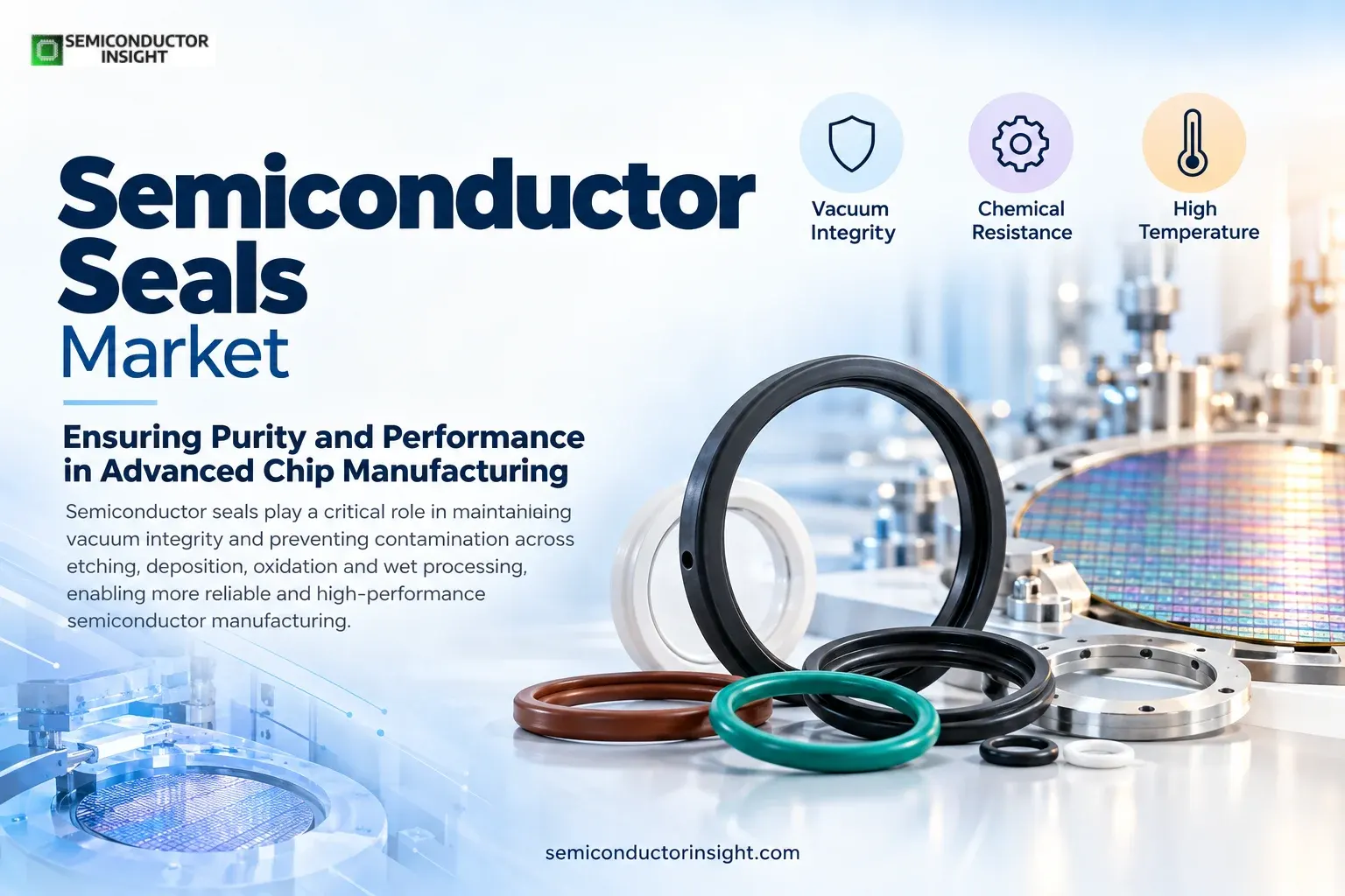
Semiconductor seals sit inside some of the most demanding environments in chip manufacturing. O-rings, door seals, valve seals, chamber seals and custom sealing components must maintain vacuum integrity while resisting plasma, fluorine-based gases, corrosive chemicals, elevated temperatures and particle generation. DuPont identifies applications spanning etching, ashing, deposition, oxidation, diffusion furnaces and wet processing, with semiconductor seals designed to limit contamination and outgassing.
The manufacturing scale behind this requirement is substantial. SEMI’s Q3 2026 outlook tracks 424 global 300 mm fabs and production lines, while installed 300 mm capacity is projected to increase 7% during 2026.
To find out more, feel free to browse our latest updated report: https://semiconductorinsight.com/report/semiconductor-seals-market/
Asia Pacific Holds the Largest Manufacturing Footprint
Asia Pacific remains the central consumption environment for semiconductor sealing technologies because it combines high-volume foundries, memory production, power semiconductor facilities and advanced packaging operations. China’s projected 300 mm capacity reaches approximately 2.4 million wafers per month in 2026, while Korea, Taiwan and Japan remain major capacity centers.
The seal requirement changes with each process. Plasma etching can expose seals to fluorine and oxygen radicals, while deposition introduces combinations of gases, temperature and vacuum. DuPont lists semiconductor sealing applications covering PECVD, PEALD, HDPCVD, conductor etch, dielectric etch and ash/strip processes, with service temperatures in several applications reaching roughly 300°C.
North America Adds New Fab and Packaging Demand
North America’s semiconductor-seal opportunity is increasingly connected with new domestic fabrication capacity. The U.S. Department of Commerce announced up to $6.6 billion in CHIPS funding for TSMC Arizona, supporting more than $65 billion of planned investment across three leading-edge fabs and a projected cluster of more than 20,000 jobs. Commerce.gov
The effect extends beyond wafer fabrication. New fabs require vacuum chambers, gas-delivery systems, valves, pumps and chemical-handling equipment, all of which depend on sealing components. Parker specifically identifies semiconductor chemical distribution systems as requiring high-integrity FFKM seals to prevent leaks and contamination. corpapps.parker.com
Europe Connects Advanced Research with Seal Qualification
Europe’s semiconductor ecosystem is developing through pilot lines as well as commercial manufacturing. In February 2026, the European Commission announced the NanoIC pilot line at IMEC Leuven with total investment of €2.5 billion, including €700 million in EU funding. The facility supports semiconductor technologies beyond 2 nm and allows companies to test equipment and processes at near-industrial scale.
France also launched the €830 million FAMES pilot line at CEA-Leti in Grenoble for ultra-low-power FD-SOI technologies. These facilities create testing environments where seal purity, vacuum performance, plasma resistance and particle behavior become important alongside the semiconductor process itself.
Latin America Builds a Smaller but Expanding Semiconductor Base
Latin America’s role is developing through electronics manufacturing, semiconductor design and government-supported technology programmes. Brazil’s Brasil Semicon programme is intended to strengthen semiconductor production, research, and innovation and design capabilities.
For seal suppliers, the regional opportunity is therefore connected to the gradual development of semiconductor and electronics infrastructure rather than the enormous wafer volumes found in East Asia. Equipment used for chemical handling, cleaning, and deposition and testing can create demand for chemically resistant sealing materials as local capabilities expand.
Middle East & Africa Move toward Semiconductor Supply-Chain Participation
The Middle East and Africa represent an emerging semiconductor ecosystem, with opportunities linked to electronics, industrial technology, advanced computing infrastructure and supply-chain diversification. SEMI’s regional outlook places Europe and the Middle East at approximately 7% of global 300 mm front-end capacity in 2026.
For semiconductor seals, growth can develop through equipment servicing, process infrastructure, specialty chemical handling and future fabrication or packaging investments. The region’s importance therefore extends beyond immediate wafer output to the supporting ecosystem needed for semiconductor manufacturing.

Comments (0)