
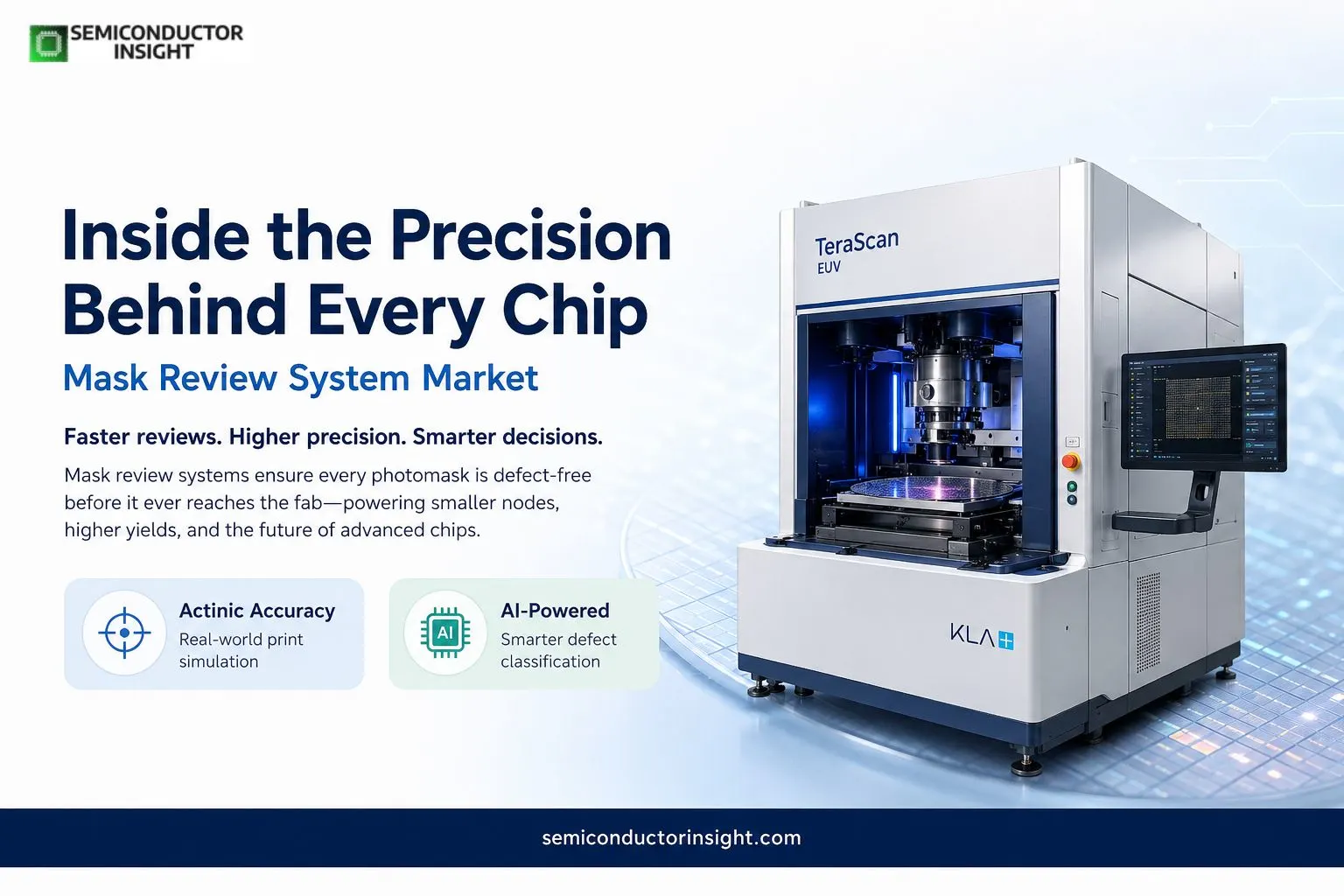
Top 15 Key Players Shaping the Future of the Mask Review System Market with Innovative Solutions and Market Expansion
Photomasks carry the circuit patterns that every advanced chip depends on. After a high-speed inspection tool flags candidate defects, a mask review system steps in to decide which ones truly matter.
These instruments capture high-resolution images or aerial images that mimic the exact optical conditions of the wafer scanner so engineers can judge printability without running a multi-day wafer print test.
KLA Corporation
Picture the quiet nerve center of every advanced mask shop: KLA’s Teron and TeraScan families sit there, scanning optical and EUV reticles for the defects that would otherwise ruin entire wafer lots. As of June 30, 2026 the company employed roughly 17,000 people across 18 major regions, supporting a backlog that climbed to $12.57 billion. Its reticle systems handle blank inspection, patterned optical masks, and EUV masks in the same workflow, feeding data into AI-driven classification engines that chipmakers now treat as essential for sub-3 nm and High-NA nodes. In calendar 2025–2026 the firm continued expanding process-control intensity for AI accelerators and advanced packaging, delivering systems that combine high-speed optical scans with e-beam review so foundries can qualify masks in hours instead of days.
Lasertec Corporation
In Yokohama a lean team of just over 1,160 employees (as of mid-2025, with continued hiring into 2026) builds the only commercially available actinic EUV mask inspection tools on the planet. Fiscal 2025 net sales reached ¥251.4 billion, driven by the ACTIS series. October 2025 brought the ACTIS A200HiT, which triples inspection speed of the earlier A150 while catching every printable defect inside wafer fabs. December 2025 added the MAGICS M9750/51 blank-inspection systems with higher sensitivity and precision stages; March 2026 launched the MATRICS X712 for 90–250 nm nodes that finishes a full mask scan in as little as 22 minutes. These tools now sit at every major EUV mask shop and an increasing number of High-NA pilot lines.
Applied Materials, Inc.
Applied Materials treats mask review as one more link in its end-to-end process-control chain. Its e-beam platforms (including ProVision-class systems) and optical tools feed directly into the same data infrastructure used for deposition and etch chambers. In 2026 the company highlighted multi-year growth in process diagnostics and control, expecting the segment to expand more than 50 percent calendar-year, partly on the strength of e-beam review for high-aspect-ratio structures and advanced packaging. Field upgrades to older ALTA laser writers keep thousands of existing mask writers productive, while new dark-field optical systems push higher throughput for intermediate process steps. The net effect is fewer tool interfaces for mask shops that already run Applied’s deposition and etch equipment.
For More Detailed Insights, You Can Surf Our Latest Report Here: https://semiconductorinsight.com/report/mask-review-system-market/
NuFlare Technology Co., Ltd.
NuFlare’s NPI-8000 and NPI-8000V optical mask inspection systems use a 199 nm laser source and finish a 6-inch mask in under 60 minutes, targeting the most advanced patterned reticles. The company, long known for its multi-beam electron-beam mask writers (MBM series), has extended the same precision optics and data-path expertise into inspection so that a single supplier can cover both writing and defect detection. Development continues for EUV and future nanoimprint-compatible tools, keeping NuFlare inside the closed loop of leading-edge mask production lines that demand both high throughput and sub-nanometer sensitivity.
Advantest Corporation
September 2025 saw Advantest release the E3660 Mask CD-SEM, engineered for 2 nm-node photomasks and EUV masks. The system improves critical-dimension reproducibility by more than 20 percent over the previous E3650 generation and adds specialized measurement modes for curvilinear patterns that are becoming common in advanced logic. Complementing it is the E5620 MASK DR-SEM, a dedicated defect-review scanning electron microscope that imports defect coordinates from any inspection tool and automatically images ultra-small defects on both photomasks and blanks. These tools target both merchant mask shops and captive mask departments inside foundries, closing the metrology loop between inspection and repair.
Carl Zeiss AG (Semiconductor Mask Solutions)
Zeiss SMT’s AIMS EUV platform remains the reference aerial-image metrology tool that emulates scanner conditions. In 2025 the company introduced the AIMS EUV 3.0, which supports both 0.33 NA isomorphic and 0.55 NA anamorphic High-NA imaging on the same system. Additional clean-room space came online in Roßdorf in autumn 2025, and a new innovation center opened in South Korea in mid-2026 to tighten collaboration with local customers. The Semiconductor Mask Solutions group develops and manufactures systems that inspect, measure, and repair photomasks, feeding directly into the same optics expertise that supplies ASML’s EUV projection lenses.
ASML (HMI division)
Through its HMI business ASML brings multi-beam e-beam technology into the mask-related workflow via wafer print-check and high-resolution defect detection. The eScan 1100, the first multi-beam system for in-line use, deploys 25 electron beams and can raise throughput up to 15 times versus single-beam tools while still resolving sub-10 nm defects. Die-to-database capability lets chipmakers monitor EUV mask printability on actual wafers, closing the loop between mask shop and fab. Installations continue to expand in 2025–2026 as High-NA pilot lines demand faster, higher-resolution review of both masks and printed wafers.
Hitachi High-Tech Corporation
Hitachi High-Tech’s GS1000 Electron Beam Area Inspection System delivers wide-area, high-resolution imaging (80 µm × 80 µm batch fields with <0.02 % uniformity) that supports both wafer and reticle-related defect detection at 5 nm and 3 nm nodes. Its long-established CD-SEM fleet more than 5,600 instruments shipped historically remains the workhorse for critical-dimension metrology, while FIB-based repair tools such as the GR3000 enable precise mask defect repair with nitrogen ion beams that leave the quartz substrate undamaged. These systems sit side-by-side with optical inspection tools in many mask shops, providing the high-resolution review step that optical scanners cannot resolve alone.
MueTec GmbH
This German specialist focuses on automated microscopy and metrology for mask and wafer applications, delivering compact optical and hybrid systems that fit into both research and production mask environments. Its tools emphasize high-precision stage control and flexible illumination for defect review and critical-dimension measurement on a range of mask materials. In the current generation of tools the company continues to support legacy and mid-node mask shops that need reliable, lower-cost review stations while still interfacing with the larger inspection platforms from KLA or Lasertec.
LAZIN Technologies Ltd.
LAZIN develops specialized optical and laser-based inspection modules used in mask blank and patterned-mask review. Its systems target high-sensitivity detection of surface and subsurface defects on quartz and other substrates, often integrated into larger process-control lines. Recent engineering work has focused on improving coordinate accuracy and reducing false positives so that smaller mask houses can achieve production-worthy quality without the capital outlay of the largest actinic platforms.
VPtek Co., Ltd.
VPtek supplies optical inspection and review equipment tailored to the Chinese and broader Asian mask-manufacturing ecosystem. Its platforms handle both blank and patterned masks, with emphasis on throughput suitable for the growing number of domestic mask shops supporting local foundries. The company continues to expand its installed base of mid-range systems that complement the high-end tools from global suppliers.
Yuweitek (Shanghai) Co., Ltd.
Yuweitek concentrates on optical and hybrid mask-inspection solutions for the Chinese semiconductor supply chain. Its systems are used for incoming and outgoing quality control of photomasks, with software that supports common database formats and defect-classification workflows. As domestic mask capacity expands in 2025–2026, Yuweitek’s tools appear in an increasing number of second-source and captive mask lines.
TENYUM Co., Ltd.
TENYUM provides specialized metrology and review instrumentation for photomask and reticle applications, focusing on high-precision optical measurement and defect imaging. Its equipment is deployed in both production and R&D mask environments where rapid, accurate review of critical features is required. The company continues to refine stage accuracy and illumination options to keep pace with tightening design rules.
Nikon Corporation
Nikon’s mask-dimension measurement systems use high-resolution i-line optics and advanced algorithms to deliver precise line-width and coordinate metrology on photomasks. The same optical expertise that produces lithography scanners is applied to dual-side coordinate measurement and video-based inspection platforms such as the NEXIV series, which now measure both two-dimensional features and height with roughly 1.5 times the throughput of earlier models. These tools serve mask shops and semiconductor makers that need non-destructive, high-accuracy dimensional control alongside the larger inspection systems.
Tokyo Electron Limited
Tokyo Electron’s process-equipment portfolio includes tools that interface tightly with mask and reticle quality control, particularly in coater/developer and related modules where mask-derived patterning integrity is verified. While primarily known for deposition, etch, and clean systems, the company continues to integrate inspection and metrology data streams that feed back into mask-related process adjustments. In 2025–2026 its focus on advanced packaging and High-NA-compatible process modules has increased the importance of closed-loop data from mask review tools upstream of the fab.

Comments (0)