
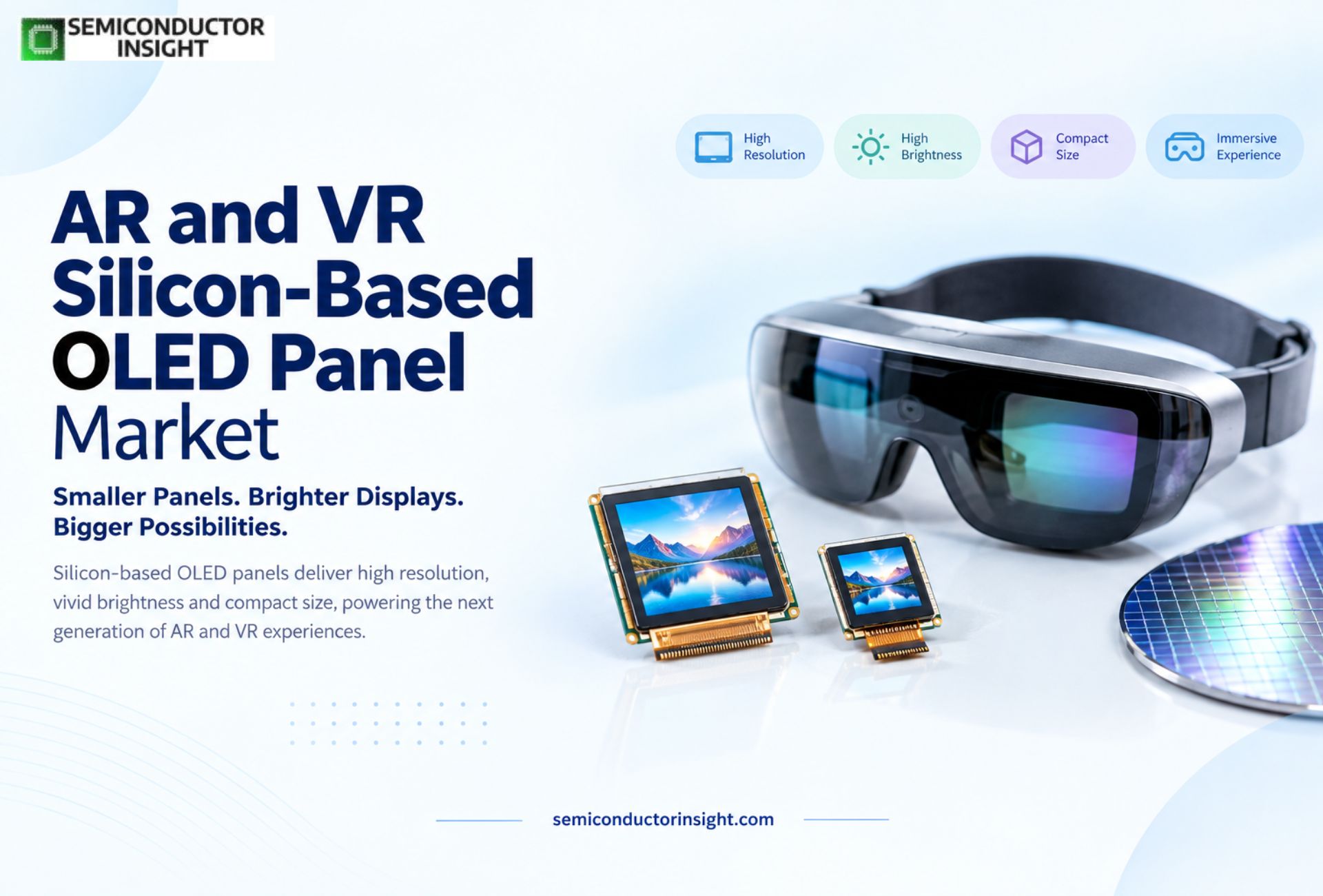
Top 10 Leading Companies in the Global AR and VR Silicon-Based OLED Panel Market in 2026
Silicon-based OLED (OLEDoS or OLED-on-silicon) microdisplays sit at the heart of modern AR and VR systems. Built on single-crystal silicon backplanes, these tiny panels deliver thousands of pixels per inch, high contrast, and the brightness needed for waveguides or immersive headsets.
Demand spans consumer smart glasses, professional training simulators, military helmets, medical viewers, and camera electronic viewfinders. The companies below shape this space through fabrication know-how, brightness breakthroughs, and production scale. Information draws from company announcements, technical presentations, press releases, and institutional reports through mid-2026.
EMagin (Samsung Display)
EMagin, acquired by Samsung Display in 2023 and operating from its Hudson Valley, New York facilities, remains a cornerstone of high-brightness RGB OLEDoS technology. Its direct-patterning and tandem-stack approaches have pushed panel performance into new territory. At Display Week and AWE USA 2026, teams demonstrated 0.62-inch and 1.3-inch panels reaching 20,000 nits and, later, prototypes hitting 40,000 nits peak brightness levels that support outdoor AR overlays and efficient waveguides. Pixel densities sit in the multi-thousand PPI range, with resolutions such as 1280 × 1024 on the smaller format.
The partnership with mask specialists has enabled sub-micron precision patterning critical for these results. Beyond consumer AR glasses demos showing real-time translation and navigation, the panels target military, medical, and industrial near-eye systems. As Samsung integrates the technology into broader production plans aiming toward higher volumes later in the decade, eMagin’s U.S. cleanroom expertise continues to anchor secure, high-performance supply for demanding applications.
Kopin
Kopin stands out as one of the few U.S.-based microdisplay specialists still fully controlling multiple technologies under one roof in Westborough, Massachusetts (with additional capabilities in Scotland). The company produces OLED, LCD, LCoS, and MicroLED microdisplays, plus a bidirectional NeuralDisplay architecture under development. In 2026 it brought OLED deposition equipment in-house to shorten lead times and strengthen defense supply chains for first-person-view drones, thermal weapon sights, pilot helmets, and soldier systems. Recent prototype work has demonstrated full-color single-panel brightness exceeding 150,000 nits in related programs.
Kopin supports IDIQ-style government contracts that can scale with demand through the end of the decade and continues to fulfill international OLED orders alongside its domestic defense focus. The multi-technology platform lets customers choose the best emitter for size, power, or environmental constraints, keeping the company relevant across both mission-critical and selected industrial near-eye uses.
Sony Semiconductor Solutions
Sony’s OLED microdisplay lineup, built on proprietary high-mobility silicon backplanes, has long set the standard for image quality in electronic viewfinders and is expanding into AR and VR headsets. Models range from 0.44-inch Full HD panels with 5.1 µm pixels (around 5,000 PPI) and peak luminance up to 10,000 cd/m² to larger 0.55-inch, 0.68-inch, and 1.30-inch formats offering WUXGA or higher resolutions and contrast ratios of 100,000:1. Frame rates reach 120 fps or more on selected devices, reducing motion artifacts in head-mounted systems. The ECX350F and related parts use novel OLED structures and microlenses to maintain brightness and uniformity at extreme pixel densities while shrinking overall module size for thinner glasses. These panels already appear in professional cameras and are finding new homes in AR glasses and VR headsets where color fidelity and low latency matter. Sony’s continuous refinement of drive circuits and compensation techniques keeps its silicon-OLED family competitive for both consumer and specialized optical systems.
Microoled
Headquartered in Grenoble, France, within the Minatec research ecosystem, Microoled designs and manufactures low-power OLED-on-silicon microdisplays for near-eye applications. The company employs roughly 50–100 people and has delivered more than one million microdisplays across its history. Its portfolio includes full-color, multi-color, and monochrome panels in sizes such as 0.19-inch, 0.38-inch, 0.39-inch, and 0.59-inch, with resolutions from several hundred thousand to over five million dots. Patented low-voltage technology supports brightness levels up to 35,000 cd/m² while emphasizing power efficiency critical for battery-powered AR glasses, sports optics, medical ocular devices, and night-vision systems. Earlier funding rounds supported capacity expansion aimed at tripling output toward 2026. Microoled also offers complete electro-optical modules, allowing customers to move from panel to integrated solution more quickly. Its European manufacturing base and focus on high-efficiency designs position it strongly for professional and outdoor near-eye markets.
Fraunhofer IPMS
As a leading independent research institute in Dresden, Fraunhofer IPMS develops and pilots OLED-on-silicon microdisplays and related sensors under one roof, covering CMOS backplane design through OLED deposition. Recent work has produced monochrome panels exceeding 70,000 nits (with test stacks above 200,000 nits) via multi-unit stacked OLED architectures, improving lifetime at high brightness. In 2026 the institute presented a 1.07-inch 2K (2048 × 2048) full-color microdisplay with 9.3 µm pixels and high-voltage backplane circuitry capable of 120 Hz refresh. Earlier transparent microdisplay prototypes reached 45 % optical transparency using clustered pixel designs suitable for see-through AR optics. The institute supplies evaluation kits, licenses technology, and supports pilot fabrication for industrial partners targeting AR data glasses, wearable systems, and high-brightness near-eye applications. Its dual expertise in circuit design and organic stack engineering continues to push the performance envelope for next-generation silicon OLED panels.
MED
MED contributes specialized silicon OLED microdisplay solutions aimed at professional and industrial near-eye systems. Its work emphasizes compact form factors and reliable performance for applications that demand consistent image quality under varied lighting. The company’s panels support the growing set of AR and VR use cases that require silicon backplanes for high pixel density and low power. By focusing on integration-ready designs, MED helps bridge laboratory advances into practical modules used in training, inspection, and specialized optical equipment. Ongoing refinements keep its offerings aligned with the brightness and resolution needs of current waveguide and immersive systems.
Oleid
Oleid develops silicon-based OLED microdisplays tailored for AR and VR near-eye optics. The company’s approach prioritizes the combination of high resolution and practical luminance levels needed for wearable devices. Its panels find roles in systems where size, weight, and power constraints are strict. Oleid’s contributions support the broader ecosystem of component suppliers feeding headset and smart-glasses manufacturers, with attention to manufacturing consistency and optical compatibility. Recent activity reflects the industry-wide push toward brighter, more efficient emitters for daylight-capable AR.
Yunnan Invensight Optoelectronics Technology Co., Ltd
Part of the expanding Chinese silicon-OLED landscape centered in Yunnan, this company participates in the production and development of OLED-on-silicon microdisplays for AR, VR, and related near-eye applications. Regional facilities have moved from earlier 8-inch lines toward higher-capacity processes, supporting volumes measured in the hundreds of thousands to millions of panels annually across the broader Yunnan cluster. Products target both consumer headsets and professional systems, benefiting from local supply-chain density and government-backed scale-up efforts. The firm’s output contributes to the rising availability of competitively priced high-PPI panels that reduce reliance on a small number of overseas suppliers.
Guozhao Tech (Nanjing Guozhao Optoelectronics)
Guozhao focuses on compact silicon OLED microdisplays and matching optical modules for AR. At industry exhibitions it has shown 0.2-inch VGA (640 × 480, 6.3 µm pixels), 0.36-inch and 0.37-inch SXGA (1280 × 1024, ~5.7 µm pixels) full-color and monochrome panels, along with waveguide modules offering 30° fields of view and resolutions such as 1280 × 720. Interfaces include MIPI and SPI, with features such as adaptive brightness and low power draw. These products suit information-overlay AR glasses and civilian viewing applications. By combining microdisplay fabrication with optical integration, Guozhao shortens the path from panel to wearable system for Chinese and international customers.
To find out more, feel free to browse our latest updated report: https://semiconductorinsight.com/report/ar-and-vr-silicon-based-oled-panel-market/
Shanghai Shiya Information Technology Co., Ltd (SeeYA / Shiya Technology)
Shiya (often associated with Hefei and Shanghai operations) has established itself as a volume leader in 12-inch wafer-based silicon OLED production the first company reported to achieve large-scale output on this larger substrate format. Its flagship 1.3-inch panels reach resolutions such as 3552 × 3552 (over 3800 PPI) with brightness around 4000 nits, while earlier lines support a range of smaller formats. Accepted capacity on the initial 12-inch line has been cited in the range of several thousand wafers per month, translating into multi-million panel annual potential once fully ramped. In 2026 the company expanded engagement with major headset makers and continued construction of additional capacity. The shift to 12-inch wafers improves die count per substrate compared with traditional 8-inch processes, supporting cost reduction and higher volume for VR and mixed-reality devices.

Comments (0)