
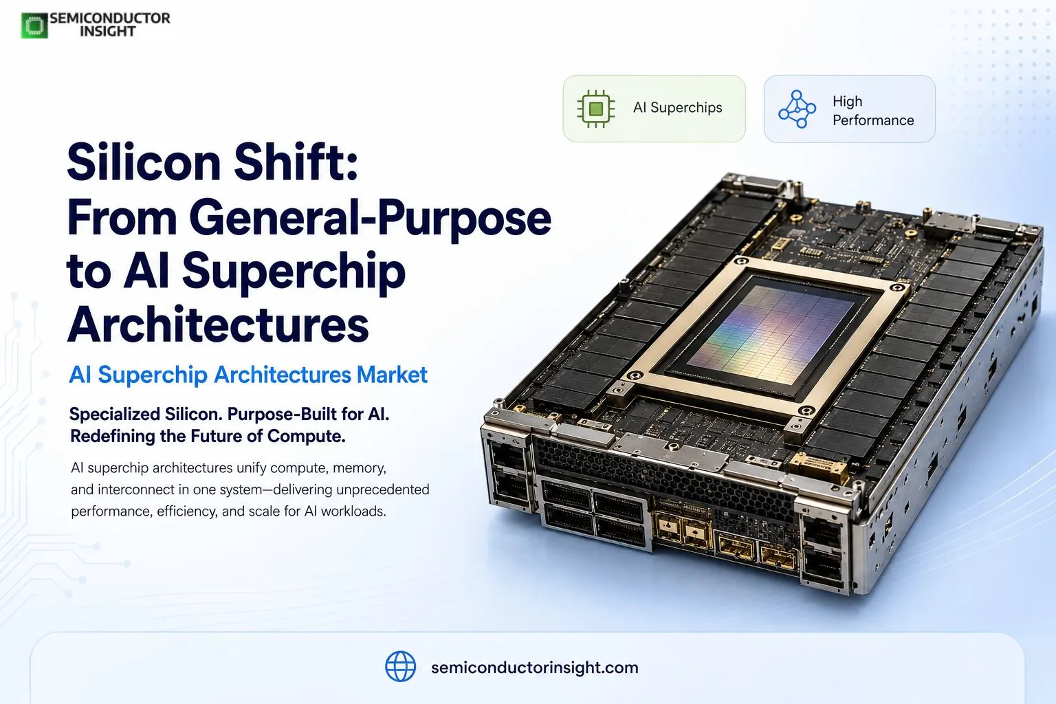
Silicon Shift From General‑Purpose to AI Superchip Architectures Market Specialization
AI Superchip Architectures Market refers to the global industry focused on the design, development, integration, and commercialization of advanced semiconductor architectures specifically engineered to handle high-performance artificial intelligence workloads.
In 2026, AI superchip architectures are no longer a niche experiment but the structural backbone of the AI silicon market, especially in data centres and large‑scale training clusters. Unlike traditional GPUs pushed into AI roles, modern superchip designs are built from the ground up around massive tensor engine arrays, high‑bandwidth memory hierarchies, and kilometer‑scale interconnect fabrics.
- For example, Nvidia’s Rubin‑family platform, built as a six‑chip architecture partly developed in Israel, treats its entire system as a single AI superchip rather than a collection of discrete processors.
- Apple’s M4‑class AI‑centric SoCs and AMD’s upcoming MI‑series AI accelerators similarly consolidate AI cores, scalar engines, and memory controllers into unified architectures, signaling a shift from generic compute to AI‑specific silicon at the architecture level.
Data Centre AI Chip Market Growth and Its Architectural Consequences
The global data centre AI chip market is witnessing a surge in both unit volumes and system complexity. Shipments of data centre AI chips are projected to grow from around 30.5 million units in 2024 to roughly 53 million units by 2030, even as individual architectures grow physically larger and more complex. This growth is propelled by hyperscalers expanding their AI capacity, with AI chip shipments such as high‑end GPUs and application‑specific AI accelerators expanding at double‑digit to triple‑digit rates in certain segments.
Architecturally, this means that AI superchip designs must balance raw tera‑ops with thermal density, power delivery, and interconnect bandwidth; otherwise, the system cannot scale beyond a few racks. The result is a new class of rack‑scale AI machines where the chip is effectively a wafer‑scale or multi‑chiplet module, tightly integrated with high‑bandwidth memory and high‑speed optical interconnects.
For a more thorough report, please contact us using our most recent report: https://semiconductorinsight.com/report/edge-ai-accelerator-card-market/
Wafer‑Scale AI Superchip Architectures and Yield‑Tolerant Design
- One of the most visible architectural shifts is the move toward wafer‑scale AI superchip architectures, exemplified by Cerebras’ WSE‑3 family.
- The WSE‑3 spans an entire silicon wafer, with an area exceeding 46,000 square millimeters and more than 4 trillion transistors, delivering around 125 petaflops of AI compute through over 900,000 AI‑optimized cores.
- To make this practical, the architecture incorporates redundant cores and routing paths and uses a fail‑in‑place strategy, allowing the chip to tolerate individual defects instead of discarding an entire wafer.
- This approach directly challenges the conventional economic model of chip‑scale designs by trading raw yield loss for enormous compute density and reduced network latency between cores.
- In AI superchip architectures market, such designs are particularly attractive for large‑scale training workloads where minimizing data movement across thousands of discrete GPUs can cut both training time and total cost of ownership.
Memory Bandwidth and Interconnect Dominance in AI Superchip Architectures
In AI superchip architectures market, memory and interconnect have become first‑order constraints, not secondary add‑ons.
For example, advanced AI systems often pair multiple AI superchip packages with stacks of high‑bandwidth memory (HBM4‑class) and co‑package optics, creating architectures where internal bandwidth exceeds 10 terabytes per second per rack.
This is essential because modern large‑language models can require petabytes of parameter traffic during training, and any bottleneck in on‑chip or off‑chip memory bandwidth quickly erodes effective FLOPS.
In 2025, several leading AI platforms shifted from treating memory as a plug‑and‑play component to designing cache hierarchies, memory controllers, and interconnect fabrics in lockstep with the tensor engines themselves. The outcome is AI superchip architectures that view the entire memory and interconnect stack as part of the compute surface, not just a supporting subsystem.
Power and Thermal Boundaries Shaping AI Superchip Layouts
Power and thermal behavior are now central to AI superchip architecture decisions. Typical AI superchip packages in data centres can consume several kilowatts per rack unit, forcing designers to rethink floor‑plan strategies, clocking schemes, and power‑delivery networks. Techniques such as dynamic voltage‑frequency scaling, spatial task‑mapping to cool regions of the die, and advanced liquid‑cooling‑ready packaging layouts are becoming standard.
In some designs, the AI superchip architecture intentionally under‑populates certain regions or uses sparse compute engines to keep localized hotspots below critical thresholds, even if it slightly reduces peak theoretical performance. From a market perspective, this means that AI superchip vendors are increasingly competing on effective watts per TFLOPS and rack‑level power efficiency rather than raw FLOPS numbers.
Edge and Robot‑Scale AI Superchip Architectures
Beyond the data centre, AI superchip architectures market is stretching into edge environments and physical AI systems such as robots, autonomous vehicles, and industrial controllers. Edge AI superchip architectures often trade raw performance for determinism, low latency, and long‑term reliability, embedding safety‑critical features directly into the instruction set and interconnect fabric. For instance, certain AI‑centric SoCs integrate multiple processor clusters, dedicated neural processing units (NPUs), and hardware‑enforced isolation domains to support concurrent AI perception, planning, and control loops. These architectures are tailored to workloads where compute must be tightly coupled with sensors and actuators, creating a new sub‑category of AI superchip designs that sit between mobile‑class SoCs and full‑scale data‑centre accelerators.
AI Superchip Architectures in the Hyperscaler Ecosystem Market
- Major hyperscalers are increasingly blending their own AI superchip architectures with established vendor platforms, creating a hybrid ecosystem market.
- Google’s Tensor Processing Units, Amazon’s Inferentia and Trainium, and Meta’s custom accelerators are all built around architectures tuned to specific AI frameworks and serving patterns, rather than generic GPU‑like compute.
- These architectures are then integrated into custom AI server stacks, where the AI superchip is one node among many specialized components, including networking, storage, and power subsystems.
- In this context, AI superchip architectures market is as much about software ecosystem lock‑in and model deployment efficiency as it is about raw silicon specs.
Vendors that can tightly couple their architecture with compilers, runtime stacks, and cloud‑native tooling find themselves at the centre of a growing AI infrastructure market dominated by AI‑native workloads.

Comments (0)