
The Science and Supply Chain Behind Semiconductor Grade High Purity Quartz Sand Market
Semiconductor Grade High Purity Quartz Sand Market sits quietly at the core of modern electronics, yet its influence stretches across everything from smartphones to satellite systems. This material is subjected to rigorous purification procedures to achieve impurity levels as low as a few parts per billion, in contrast to regular industrial sand. Because semiconductor production, where circuits are etched at nanometre scales, can be disrupted by even a trace of contamination, this level of refinement is crucial.
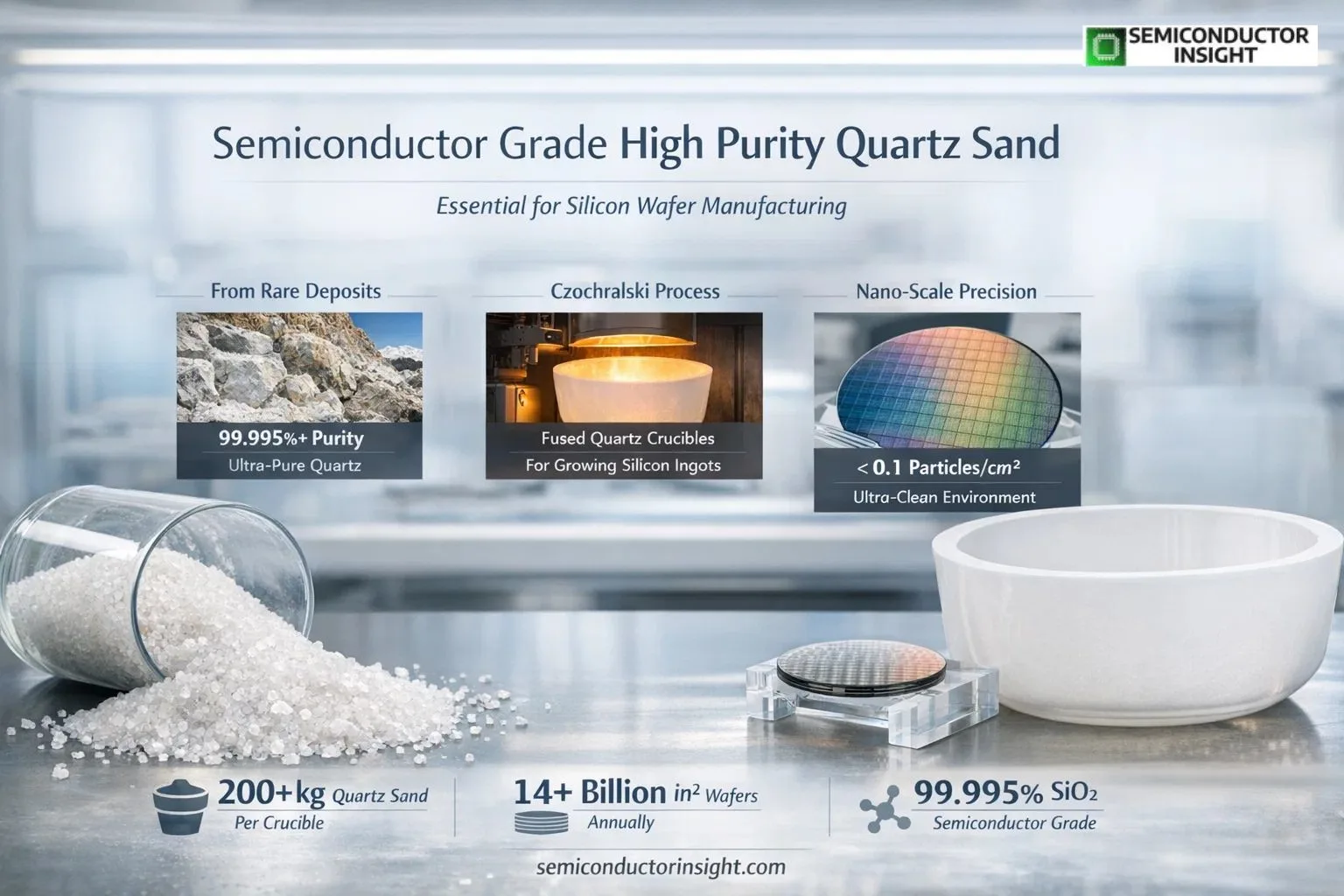
High purity quartz is primarily used to manufacture quartz crucibles, which are essential for growing silicon ingots through processes such as the Czochralski method. A single silicon wafer, often 300 mm in diameter, requires a highly stable and contamination-free environment, making quartz sand a non-negotiable input. With global semiconductor wafer production exceeding 14 billion square inches annually, the demand for ultra-pure quartz continues to scale alongside the digital economy.
From Natural Deposits to Ultra-Clean Material
- What makes semiconductor-grade quartz unique is not just its purity but its origin. Only a handful of locations globally produce quartz deposits suitable for semiconductor applications. For instance, certain mines in the United States and Norway are known for their exceptionally pure quartz, with silicon dioxide content exceeding 99.9%.
- The transformation process involves multiple stages, including crushing, washing, magnetic separation, acid leaching, and thermal processing.
- During acid leaching, strong acids remove metallic impurities such as iron, aluminum, and titanium elements that can interfere with semiconductor conductivity. After purification, the material is melted at temperatures above 1,700°C to form fused quartz, which is then shaped into components used in chip manufacturing.
- Interestingly, producing just one high-quality quartz crucible can require over 200 kg of refined quartz sand, highlighting the scale of material consumption behind each batch of semiconductor wafers.
Precision Meets Performance in Semiconductor Fabrication
The importance of quartz sand becomes even clearer when examining its role in fabrication environments. Quartz components are used extensively in diffusion tubes, wafer carriers, and etching chambers due to their ability to withstand high temperatures and resist chemical corrosion.
For example, during oxidation processes, wafers are exposed to temperatures exceeding 1,000°C in quartz furnaces. Any impurity in the quartz could introduce defects into the silicon lattice, leading to reduced chip performance or failure. This is particularly critical for advanced nodes below 10 nanometers, where even atomic-level inconsistencies can impact yield rates.
A notable instance is the production of memory chips, where manufacturers rely on ultra-clean quartzware to maintain defect densities below 0.1 particles per square centimeter. This level of precision underscores why semiconductor-grade quartz is not just a raw material but a performance enabler.
You can freely browse our most recent updated report to learn more about it before scrolling further: https://semiconductorinsight.com/report/global-semiconductor-grade-high-purity-quartz-sand-market/
Premium Quartz Standards for Semiconductor Manufacturing Success
- High purity quartz sand is not the same as regular silica. It is an ultra-refined form of silicon dioxide with a purity threshold that often exceeds 99.9% SiO₂, and at the semiconductor grade, manufacturers seek materials reaching 99.995% to 99.9% notations referred to in the industry as 4N5 through 5N.
- High-purity quartz can be processed and purified to get silicon dioxide with a purity of at least 99.995%. This is because it can withstand high temperatures, resist corrosion, expand less when heated, insulate well, and let light through. This makes it useful for high-tech industries like photovoltaics and semiconductors.
- Semiconductor-grade HPQ is different from regular industrial sand in that it has to go through a lot of tests to find trace impurities like iron, aluminum, and alkali metals. Any of these can make chips work worse in ways that are hard to see until after they are made.
- Fused quartz crucibles are one of the only parts that can be used with the Czochralski process to grow single crystal silicon ingots because they don’t expand much and can handle sudden changes in temperature quite well.
- Quartz crucibles also have the extra benefit of being non-conductive, having a nominal resistance of 1×10⁸ Ω·m at 1000°C. This makes them indispensable in the silicon wafer manufacture process, which is the first step that gives every modern chip its crystalline base.
- High-purity quartz is also used to make quartz tubing and ingots, which are part of the larger quartzware ecosystem that can be found in semiconductor production lines.
The Silent Enabler of the Digital Age
While it rarely makes headlines, semiconductor-grade high purity quartz sand is indispensable to the functioning of modern technology. Its journey from rare geological deposits to precision-engineered components reflects a blend of natural resource scarcity and advanced industrial processing.
As industries continue to demand faster, smaller, and more efficient electronic devices, the role of this material will only become more critical. In many ways, Semiconductor Grade High Purity Quartz Sand Market is not just supporting innovation it is quietly defining its limits.

Comments (0)