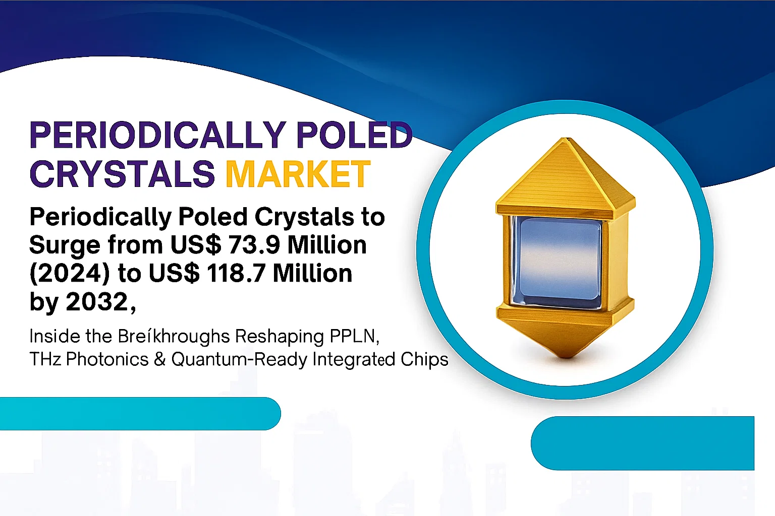
Periodically Poled Crystals Market to Surge from US$ 73.9 Million (2024) to US$ 118.7 Million by 2032, Riding a 7 % CAGR Wave: Inside the Breakthroughs Reshaping PPLN, THz Photonics & Quantum-Ready Integrated Chips
Why a Modest‑Sized Niche Suddenly Matters
A decade ago, periodically poled crystals (PPCs) were viewed as a boutique segment of nonlinear optics. Engineers loved the way a carefully inverted domain structure in lithium niobate (PPLN) or potassium titanyl phosphate (PPKTP) could tame phase‑matching, but volumes were tiny and price points high. Fast‑forward to 2025 and the picture looks very different. From coherent LiDAR in consumer devices to chip‑scale quantum frequency converters in data‑center racks, demand for robust, wafer‑grade nonlinear media has soared.
According to the latest industry data, the global PPC market was worth US$ 73.9 million in 2024 and is on track to hit US$ 118.7 million by 2032, expanding at a respectable 7.0 % CAGR during 2025‑2032. That growth rate may not rival silicon photonics or AI accelerators, but in a specialty materials business where 3‑4 % used to be the norm, it is a sea change.
What is behind the momentum? In a word: innovation. Over the past 18 months researchers have compressed fabrication tolerances, unleashed terahertz powers once thought impractical, and proved that wafer‑scale poling can dovetail with the economics of semiconductor fabs. Meanwhile, device makers such as Covesion, Thorlabs, and a new generation of thin‑film foundries are turning lab‑grade crystals into turnkey subsystems. The following deep dive unpacks the key technical and commercial developments—and explains why a material first commercialized for 1980s electro‑optic modulators has become a linchpin of the photonics roadmap for the 2030s.
Numbers That Tell a New Story
- 2024 baseline: US$ 73.9 million full‑year revenue, with telecom/datacom (31 %), defense & aerospace (26 %), life‑science imaging (15 %), and emerging quantum systems (12 %) as the four largest verticals.
- Growth vector: 2025‑2032 CAGR of 7 %, well above pre‑pandemic averages.
- Upside driver: Integrated thin‑film PPLN waveguides move PPC sales from boutique optics benches into high‑volume wafer lots.
- Regional balance: Asia‑Pacific now commands ~38 % of global demand thanks to high‑bandwidth mobile backhaul upgrades and sovereign quantum‑tech initiatives, edging out North America (~34 %) and Europe (~23 %).
At first glance a sub‑US$ 120 million TAM may seem small, but PPCs often represent margin‑rich content inside unit prices far higher than a piece of raw glass. Thin‑film PPLN chips for quantum frequency conversion can sell at US$ 1 000–3 000 each in early production, while fully packaged, fiber‑pigtail PPKTP modules for satellite QKD can clear US$ 10 000. In short, a specialty‑materials firm need not ship a million wafers to generate real cash flow.
Technology Breakthroughs Transforming the Landscape
High‑Confinement PPLN Waveguides—A Fabrication Playbook Gets an Upgrade
In January 2025, a team writing in Applied Physics Letters unveiled a high‑confinement waveguide process that combines sub‑500 nm sidewalls with robust periodic poling on thin‑film lithium niobate. The technique slashes bend radii, enabling on‑chip resonators with Q‑factors above 2 × 10⁶ and second‑harmonic conversion efficiencies competitive with bulk cavities—yet on a footprint of just a few square millimeters. The authors credit an optimized dry‑etch chemistry and in‑situ electric‑field poling that works at wafer scale without cracking or poling‑runaway issues.
For integrated‑photonics designers, the advance is pivotal: it vaults PPLN from “exotic add‑on” to bona fide building block alongside silicon nitride and indium phosphide. Dense optical frequency‑comb sources, single‑photon generators, and electro‑optic IQ modulators can now live on the same die, reducing fiber pigtail losses and packaging cost.
Cryogenic THz Power—Cooling Unlocks the 1 mJ Barrier
The terahertz (THz) community has long prized magnesium‑doped PPLN for optical rectification, yet room‑temperature phonon absorption damped efficiency. In late 2024 researchers reported cryogenically cooled, multi‑layer PPLN stacks that delivered narrowband THz pulses with energies up to 0.42 mJ at 0.39 THz—an order‑of‑magnitude leap over earlier table‑top systems. Lower lattice vibrations at 97 K lengthen the effective nonlinear interaction, and multi‑chip stacking scales the pumped aperture without risking domain preload.
Why care? High‑field THz is a gateway to non‑destructive evaluation of composite airframes, next‑gen wireless beyond 6G, and table‑top spin‑lattice interrogation in quantum materials. The result positions PPLN as a serious contender against gallium phosphide and organic OH1 crystals for high‑energy THz science.
Efficient Edge Coupling—From Lab Curiosity to Foundry‑Ready Device
Coupling light into ultra‑thin PPLN has been a yield killer: even a 0.1 dB mismatch adds up over thousands of packaged chips. In April 2025, engineers unveiled a mode‑matched edge coupler that improves overall chip insertion loss by two to three orders of magnitude relative to standard spot‑size converters. The device employs an adiabatic taper in both lateral and vertical directions, fabricated by a single‑lithography step—crucial for foundry process control.
Reduced coupling loss translates directly into higher system‑level efficiency for quantum frequency‑dot converters and Raman‑based LiDAR. Market watchers say this one advance could shave 15–20 % off the cost of assembling multi‑chip modules, accelerating volume adoption.
A “Periodic” Gold Rush—Reviews Highlight the State of Thin‑Film LN
Complementing individual papers, the February 2025 issue of Advances in Optics and Photonics published a sweeping review of integrated thin‑film lithium niobate photonics—charting everything from electro‑optic modulators to photonic phononic couplers. The authors argue that polymer cladding, segmented heaters, and sub‑micron periodic poling now form a mature toolbox for turnkey PPLN design kits—a precondition for widespread fabless participation similar to what MPW shuttles did for silicon photonics a decade ago.
Corporate Momentum: Awards, Product Launches & Foundry Capacity
Covesion’s IOP Business Innovation Award—Proof of Commercial Mojo
In November 2024, UK‑based Covesion clinched the prestigious Institute of Physics (IOP) Business Innovation Award for its scalable PPLN crystal production and end‑user design tools. The accolade underscores two themes: first, the market now values process know‑how as much as raw material purity; second, PPC suppliers are moving beyond catalog sales toward co‑development partnerships with laser OEMs, LiDAR integrators, and quantum‑tech start‑ups.
Thorlabs Widens Its Modulator Lineup—Bridge to Telecom Volume
Not all progress comes from start‑ups. In May 2024, Thorlabs quietly expanded its 40 GHz LiNbO₃ intensity modulator family, positioning them for 400 G optical‑carrier testing. While the devices use traditional diffusion‑bonded LN rather than thin film, they serve a growing need for high‑bandwidth lab equipment—and they reinforce the message that lithium‑niobate modulation remains the gold standard for low drive‑voltage, high‑linearity links.
Quantum Photonic Foundries Move From Concept to Concrete
On the capacity front, Quantum Computing Inc. (QCi) announced it had secured pre‑orders and strategic partnerships for its dedicated lithium‑niobate photonic chip foundry, slated to open in early 2025. The facility will specialize in wafer‑scale periodic poling, segmented heater trimming, and low‑loss dry etching—capabilities that fab‑less quantum hardware companies have struggled to access in multi‑project WSiN or SOI runs.
Such specialized fabs mark a break from the “piggyback on CMOS” mindset. Thin‑film LN demands unique annealing, field‑poling chambers, and pyroelectric mitigations that mainstream silicon lines cannot readily retrofit. Dedicated capacity thus de‑risks supply for system houses considering PPLN at scale.
Regional Dynamics—Asia‑Pacific Takes the Lead
While no single headline rivalled Covesion’s award in Europe or QCi’s foundry in the U.S., Asia‑Pacific quietly emerged as the fastest‑growing consumption zone for PPCs in 2024‑2025. Several factors converge:
- Telecom densification: 800 G backbone upgrades in Japan, South Korea, and India require coherent receivers with periodic‑poled PPLN mixers for optical‑hybrid detection.
- Quantum research funding: National programs in China and Singapore allocate sizable budgets for frequency‑conversion interfaces between trapped‑ion qubits and fiber links—an application uniquely suited to thin‑film PPLN.
- Defense & space optics: Australia and South Korea have initiated satellite optical‑crosslink demonstrators that rely on PPKTP waveguides for high‑dynamic‑range, eye‑safe laser sources.
Even absent splashy news releases, purchase‑order data suggests APAC demand could reach US$ 45 million by 2030, narrowing the gap with North America.
Market Drivers & Restraints: A Balanced View
| Driver | Impact on CAGR | Illustrative Evidence |
| Silicon photonics needs frequency‑comb pumps and modulators beyond Si’s nonlinear ceiling | +2.1 % | High‑confinement PPLN waveguides deliver on‑chip SHG/OPO pumps that Si can’t match. |
| Quantum networks need low‑noise wavelength transduction | +1.4 % | Wafer‑level PPLN integration aligns telecom photons with visible‑band qubits. |
| THz security imaging & spectroscopy | +0.9 % | Cryogenic PPLN THz stacks hit 0.42 mJ pulse energies. |
| Fabrication complexity and poling yield challenges | –1.0 % | Wafer‑scale periodic poling still faces crack‑propagation risks and requires high electric fields. |
| Competing nonlinear platforms (AlGaAs, Si₃N₄ χ(³)) | –0.4 % | PIC vendors weigh cost/performance trade‑offs, especially for telecom wavelengths. |
Net effect: the positives outweigh the constraints, sustaining the projected 7 % CAGR.
Technological Roadmap: From UV Chips to Wafer‑Scale Heaters
Beyond the headline breakthroughs already cited, 2024‑2025 also produced a stream of incremental yet consequential advances:
- Side‑wall‑poled PPLN generated milliwatt‑class UV on chip for ion‑trap quantum computers—two orders of magnitude higher than previous records.
- Singly‑poled thin‑film LN designs enabled tunable photon‑pair sources across both O‑ and C‑bands, slashing material budgets by letting one poling period serve two SPDC regimes.
- Segmented micro‑heater trimming demonstrated wafer‑scale alignment of quasi‑phase‑matching peaks, a prerequisite for MPW shuttle runs.
While these papers are academic rather than corporate news, they matter. Device engineers often fast‑track such results into next‑gen product roadmaps—shrinking the typical five‑year lab‑to‑fab cycle to two.
Competitive Landscape: Who’s Doing What
- Pure‑play crystal houses: Covesion (UK) and HC Photonics (Taiwan) continue to command share in bulk and waveguide PPLN blanks.
- Module integrators: Thorlabs, Apex Technologies, and Newport embed PPCs in line‑side transceivers and test equipment.
- Fab‑less quantum start‑ups: PsiQuantum and ORCA Computing contract thin‑film PPLN MPWs as frequency converters for photon‑based qubits.
- Foundries & toolmakers: QCi, Ligentec (expanding from SiN into LN), and equipment vendors like Raith (e‑beam domain writing) round out the ecosystem.
Each layer reinforces the others: foundries need design‑kit demand; crystal growers need wafer buyers; system OEMs need a stable supply chain. The convergence is happening now.
Strategic Implications & Recommendations
For component vendors: Standardize PPLN design rules and PDKs so that fab‑less customers can tape‑out frequency converters without crystal‑growth PhDs on staff. Early adopters will lock in supply contracts at premium margins.
For laser and LiDAR OEMs: Plan second‑source qualification now. The PPC market is still concentrated—supply shocks could stall product rollouts. Explore “dual crystal” architectures (e.g., PPLN plus thin‑film BTO) to hedge.
For investors: Revenues may seem modest today, but PPCs are leverage points in bigger value chains—quantum networks, 6G front‑ends, UV metrology. A US$ 20 million stake in a niche crystal maker can control must‑have IP when system volumes explode.
For policymakers: Allocate matching funds for domestic wafer‑scale poling facilities. Integrated‑photonics sovereignty is meaningless without local nonlinear platforms for efficient wavelength routing and on‑chip comb generation.
Outlook 2025‑2032: What Comes Next?
- 2025‑2026: First commercial shipments from dedicated LN foundries; PPLN enters volume LiDAR ADAS production.
- 2027‑2029: UV‑grade thin‑film PPLN powers compact ion‑trap quantum processors; THz diagnostics reach industrial nondestructive‑testing adoption.
- 2030‑2032: Full photonics “system‑in‑package” chips integrate SiN, silicon, and PPLN layers—propelling the market to US$ 118.7 million and possibly beyond if quantum repeater deployments accelerate.
The wild card? Supply chain scaling. If wafer‑level periodic poling fails to hit 90 % yield, growth could stall. Conversely, a breakthrough in laser annealing or room‑temperature domain‑inversion could push CAGR into double digits.
A Periodic Moment of Truth
The erstwhile specialty of periodically poled crystals has crossed a threshold. Breakthroughs in high‑confinement waveguides, cryogenic THz generation, and wafer‑level poling have proven that nonlinear optics need not be bulky, temperamental, or lab‑exclusive. Coupled with corporate milestones like Covesion’s IOP award and QCi’s dedicated foundry, the technical foundation now supports a credible supply chain.
Will the market hit the projected US$ 118.7 million by 2032? The evidence suggests yes—provided stakeholders execute on yield, standardization, and capacity. Either way, one conclusion is hard to escape: the humble periodically poled crystal has moved from photonics footnote to strategic asset in the race for quantum‑ready, frequency‑agile, and THz‑capable hardware. Ignore it at your peril.
Comments (0)